

Wafer transfer robot and semiconductor device manufacturing equipment comprising the same
a technology of wafer transfer robot and semiconductor device, which is applied in the direction of manipulators, cutting heads, electrical devices, etc., can solve the problems of low coefficient of friction between the wafer and the blade, the inertia of the wafer mounted on the blade, and the time-consuming of single-wafer processing
- Summary
- Abstract
- Description
- Claims
- Application Information
AI Technical Summary
Benefits of technology
Problems solved by technology
Method used
Image

Examples
Embodiment Construction
[0025]The present invention will now be described more fully hereinafter with reference to the accompanying drawings. Note, like numbers designate like elements throughout the drawings.
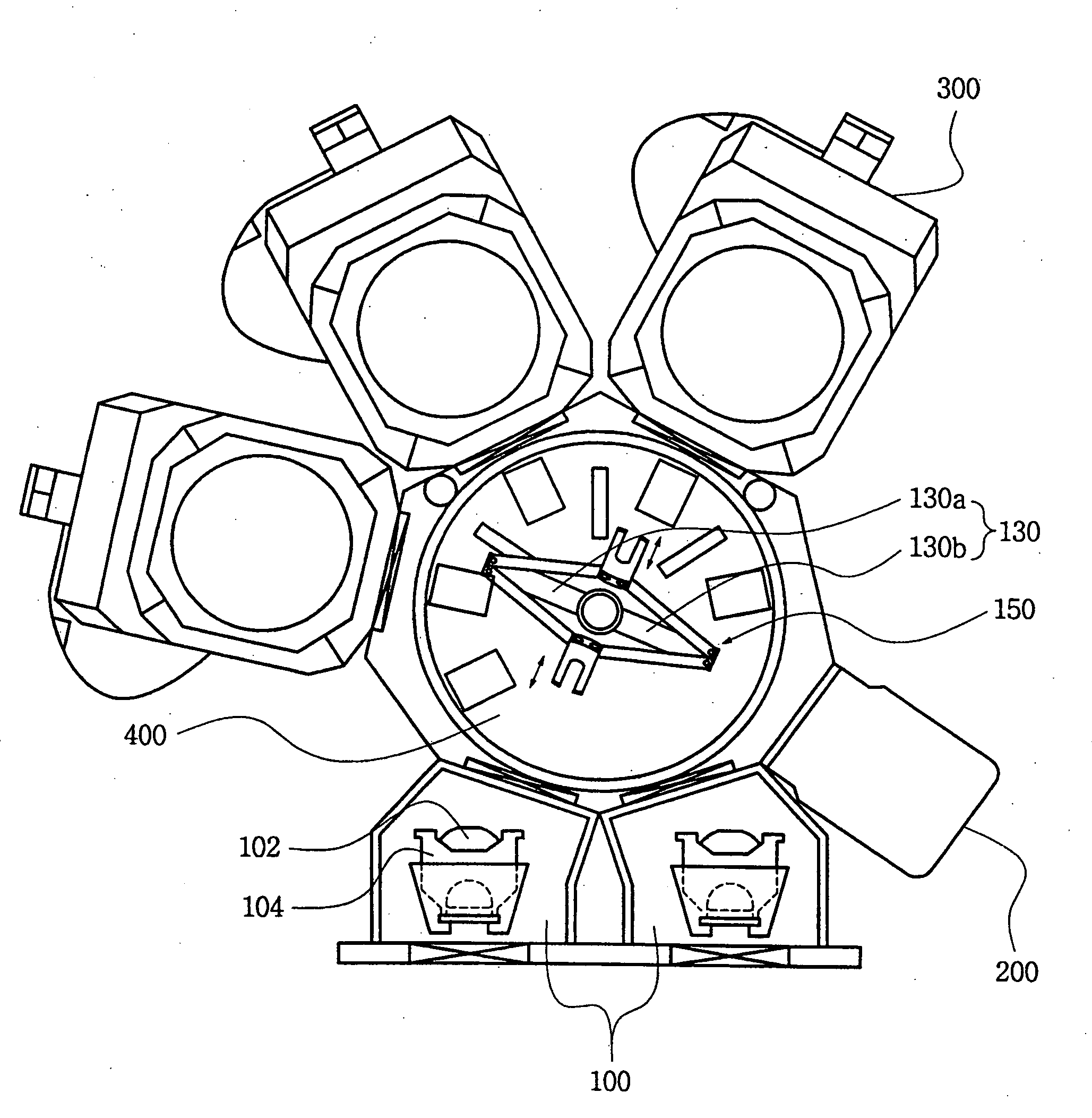
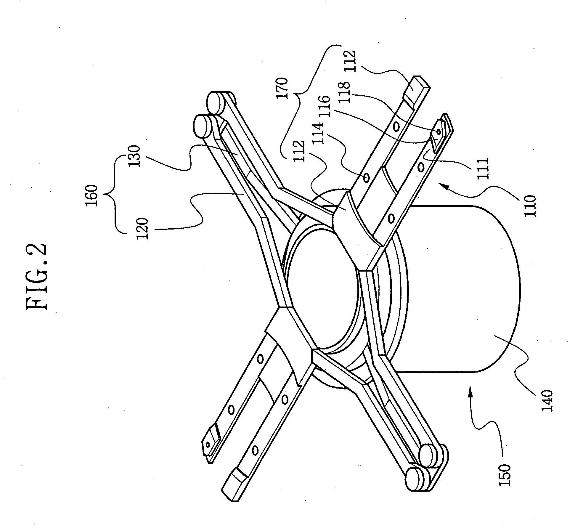
[0026]As illustrated in FIGS. 1 and 2, semiconductor device manufacturing equipment according to the present invention includes a plurality of load-locks 100 each comprising a chamber accommodating a cassette 104 in which a plurality of wafers 102 are mounted, an alignment apparatus 200 which aligns wafers 102 transferred from the load-lock chambers 100, at least one process apparatus 300 for performing a semiconductor device manufacturing process, a transfer chamber 400 to which the process apparatus 300, the alignment apparatus 200, and the load-locks 100 are commonly connected, and a wafer transfer robot 150 disposed in the transfer chamber 400. The wafer transfer robot 150 has at least one blade 110 that transfers a wafer 102 between the chambers of the load-lock and process apparatus 100 and 300....
PUM
 Abstract
Description
Claims
Application Information