Ild layer with intermediate dielectric constant material immediately below silicon dioxide based ild layer

a technology of dielectric constant and ild layer, which is applied in the direction of semiconductor devices, semiconductor/solid-state device details, electrical apparatus, etc., can solve problems such as failures during fabrication, and achieve the effect of reducing the likelihood of failure and adequate electrical properties

Inactive Publication Date: 2007-08-16
GLOBALFOUNDRIES INC
View PDF10 Cites 5 Cited by
  • Summary
  • Abstract
  • Description
  • Claims
  • Application Information

AI Technical Summary

Benefits of technology

[0006] An integrated circuit (IC) chip and related package are disclosed including a first interlevel dielectric (ILD) layer(s) including an ultra low dielectric constant (ULK) material, a second ILD layer(s) including a silicon dioxide (SiO2) based dielectric material above the first ILD layer(s), and a transitional ILD layer including an intermediate dielectric constant material. The transitional ILD layer is positioned directly below a lowermost one of the second ILD layer(s), excepting any isolation layer, which represents the layer most susceptible to failure. The intermediate dielectric constant material can have a dielectric constant and an elastic modulus greater than that of the ULK material and less than that of the SiO2 based dielectric material. Hence, the intermediate dielectric constant provides adequate electrical properties, but also absorbs more of the stress than the typical ULK material, which reduces the likelihood of failure. A method of forming the IC chip is also disclosed.

Problems solved by technology

As the integrated circuit industry continues to drive toward reduced feature size one of the challenges is maintaining the structural reliability relative to chip package interactions.
Failure may occur during fabrication (as yield losses), during testing (qualification fails) and, as a worst case scenario, during operation in the field.

Method used


Image

  • Ild layer with intermediate dielectric constant material immediately below silicon dioxide based ild layer
  • Ild layer with intermediate dielectric constant material immediately below silicon dioxide based ild layer
  • Ild layer with intermediate dielectric constant material immediately below silicon dioxide based ild layer

Examples


Embodiment Construction

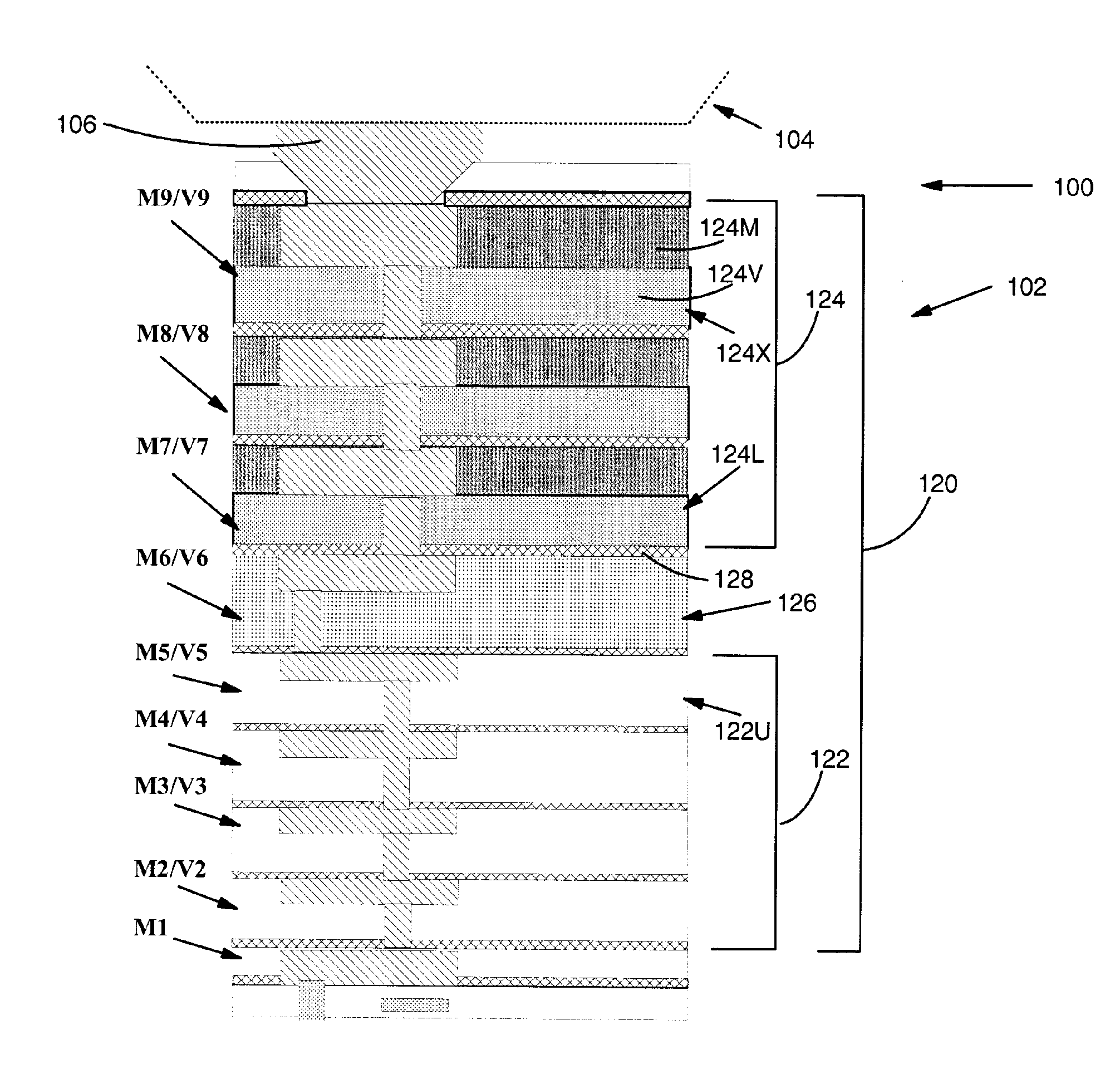
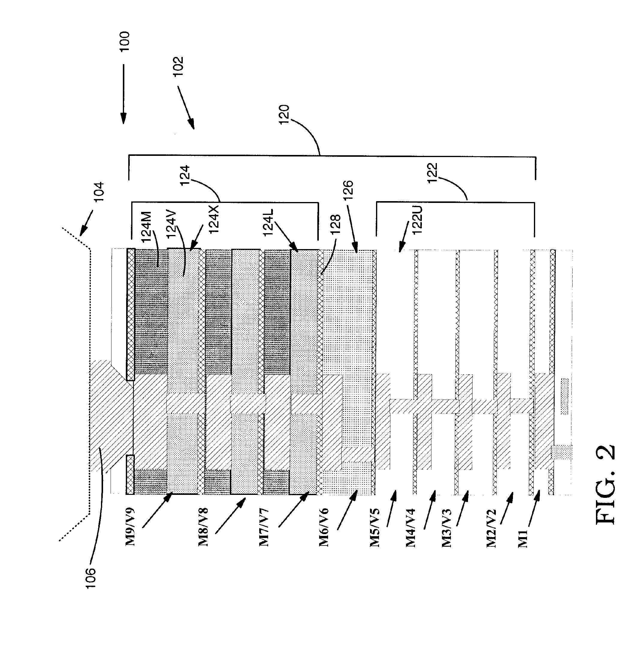
[0016] Referring to FIG. 2, one embodiment of an integrated circuit (IC) chip package 100 including an integrated circuit (IC) chip 102 is illustrated. IC chip package 100 also includes a substrate 104 and interconnections 106 (one shown). Substrate 104 may include any now known or later developed circuit board substrate material, such as those including an organic laminate. Substrate 104 may have a coefficient of thermal expansion (CTE) of approximately 6 parts per million per degree Celsius (ppm / ° C.), and typically 15-18 ppm / ° C. IC chip 102 may have a CTE of approximately 3 ppm / ° C. Interconnections 106 may include any now known or later developed electrically conductive interconnections or wire bond connections, e.g., ball grid arrays, etc., between substrate 104 and IC chip 102.

[0017] IC chip 102 includes a multi-level interconnect structure 120 according to one embodiment of the invention. Multi-level interconnect structure 120 includes at least one first interlevel dielectr...


PUM


Abstract

An integrated circuit (IC) chip and related package are disclosed including a first interlevel dielectric (ILD) layer(s) including an ultra low dielectric constant (ULK) material, a second ILD layer(s) including a silicon dioxide (SiO2) based dielectric material above the first ILD layer(s), and a transitional ILD layer including an intermediate dielectric constant material. The transitional ILD layer is positioned directly below a lowermost one of the second ILD layer(s), excepting any isolation layer, which represents the layer most susceptible to failure. The intermediate dielectric constant material can have a dielectric constant and an elastic modulus greater than that of the ULK material and less than that of the SiO2 based dielectric material. Hence, the intermediate dielectric constant provides adequate electrical properties, but also absorbs more of the stress than the typical ULK material, which reduces the likelihood of failure. A method of forming the IC chip is also disclosed.

Description

BACKGROUND OF THE INVENTION [0001] 1. Technical Field [0002] The invention relates generally to integrated circuit fabrication, and more particularly, to an integrated circuit chip, a related chip package and method that provide an intermediate dielectric constant material at an interlevel dielectric (ILD) layer directly below a silicon dioxide (SiO2) based dielectric material to reduce stress in back-end-of-line layers. [0003] 2. BACKGROUND ART [0004] As the integrated circuit industry continues to drive toward reduced feature size one of the challenges is maintaining the structural reliability relative to chip package interactions. Chip package interactions include structural interactions between multi-level interconnect structures (referred to as back-end-of-line (BEOL) layers and including all layers after a first metal (M1) layer) of a chip, interconnections between the chip and substrates. Conventional BEOL layers require more fragile low dielectric constant (low-k) dielectric...

Claims


Application Information

Patent Timeline
Patent Type & Authority Applications(United States)
IPC IPC(8): H01L23/52
CPCH01L21/76801H01L23/5329H01L23/53295H01L2924/0002H01L2924/00
Inventor FAROOQ, MUKTA G.HANNON, ROBERTMELVILLE, IAN D.ZUPANSKI-NIELSEN, DONNA S.
Owner GLOBALFOUNDRIES INC
Why Eureka
Try Eureka