HIGH k GATE STACK ON III-V COMPOUND SEMICONDUCTORS

a compound semiconductor and high k gate technology, applied in the field of semiconductor structure, can solve the problems of poor interface between high k dielectric and gaas semiconductor material, lack of natural oxide, and impede the development of standard metal oxide semiconductor devices, etc., and achieve low interface state density, good quality, and sufficient electrical properties.

Active Publication Date: 2012-12-27
GLOBALFOUNDRIES U S INC
View PDF3 Cites 18 Cited by
  • Summary
  • Abstract
  • Description
  • Claims
  • Application Information

AI Technical Summary

Benefits of technology

[0015]The present invention provides a method in which a high k dielectric material having a dielectric constant of greater than that of silicon dioxide can be formed on a surface of a III-V compound semiconductor material with electrical properties sufficient for high-performance FET applications wherein the interface between the high k dielectric material and the III-V compound semiconductor material is of good quality, resulting in a low interface state density (on the order of about 1012 cm−2 eV−1 or less); the unit for the interface state density can also be written as cm−2 / eV. That is, the present invention provides a method in which a high k dielectric material is formed on an unpinned, i.e. passivated, surface of a III-V compound semiconductor material. In accordance with the method of the present invention, the surface of the III-V compound semiconductor includes substantially no oxide or other contaminants that would otherwise cause a large interface state density in the structure.
[0031]The methods of the present invention described above have has several advantages. First the semiconducting, e.g., Si, layer is excellent at passivating a surface of a III-V compound semiconductor material, particularly a GaAs surface. Secondly, by depositing the semiconducting layer using a high-quality technique such as MBE, the surface can be cleaned (either by desorbing the oxygen at high temperatures, or using a H-plasma preclean), to create a virtually oxygen-free interface. The semiconducting layer thickness can be controlled to high precision as well, and thus be made very thin. If the semiconducting layer is nitridated, in situ, a nitrogen plasma could be used to then convert the semiconducting layer to a semiconducting nitride. Nitride, instead of oxide, formation has the advantage that over nitridation will not cause problems, as generally, nitridation of the GaAs surface does not degrade the electrical characteristics. Over oxidation, on the other hand, can severely degrade the electrical characteristics. Once the nitride is formed, the surface is stable against oxidation, and could be removed and exposed to air, for subsequent high k deposition. A semiconducting nitride also has the advantage of allowing the subsequent HfO2 that is deposited to nucleate amorphous as opposed to polycrystalline, which can improve the electrical properties. The HfO2 could be deposited in situ as well, which would have the advantage that the entire gate stack could be deposited in a single vacuum step. The inventive process has the additional advantage that it does not require a high-temperature step, as the H-preclean, semiconducting layer deposition, optional nitridation, oxidation or oxynitridation and high k deposition all could be performed at a temperature of less than 300° C., which would avoid any contamination or surface degradation problems associated with sublimation of one of the elements of the III-V compound semiconductor material.

Problems solved by technology

One major disadvantage of a GaAs semiconductor material (as well as the other III-V compound semiconductors) is the lack of a natural oxide.
This feature hinders the development of standard metal oxide semiconductor (MOS) devices that require the ability to form a surface dielectric.
Moreover, when a dielectric material having a dielectric constant that is greater than silicon dioxide (k greater than 4.0) is deposited on a GaAs semiconductor material that has an unpassivated surface, the interface between the high k dielectric and the GaAs semiconductor material is typically poor, resulting in a high interface state density (on the order of about 1013 cm−2 eV−1 or greater).
Because of such a high interface state density, the electrical properties of the dielectric are insufficient for use with high-performance FETs.
Several known solutions have been proposed, but each have problems / drawbacks associated therewith.
However, it requires a complex dual chamber molecular beam epitaxial (MBE) system which is not suitable for manufacturing.
Moreover, Ga2O3 has the problem that it has a relatively low bandgap, and therefore can produce higher leakage than is desirable for scaled MOSFET applications.
Both of these techniques mentioned in the above articles have the problem that an III-V MBE chamber is needed to first produce a high-quality GaAs interface before Si deposition.
In addition to the above-mentioned techniques, several techniques have been purposed to passivate a GaAs surface, yet these techniques have not been utilized in conjunction with a high k dielectric.

Method used


Image

  • HIGH k GATE STACK ON III-V COMPOUND SEMICONDUCTORS
  • HIGH k GATE STACK ON III-V COMPOUND SEMICONDUCTORS
  • HIGH k GATE STACK ON III-V COMPOUND SEMICONDUCTORS

Examples


example

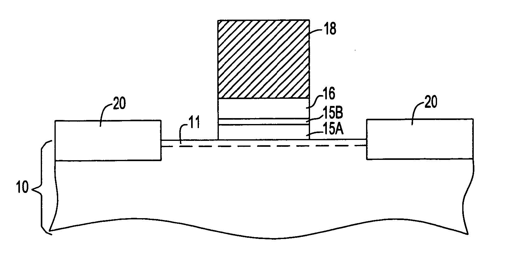
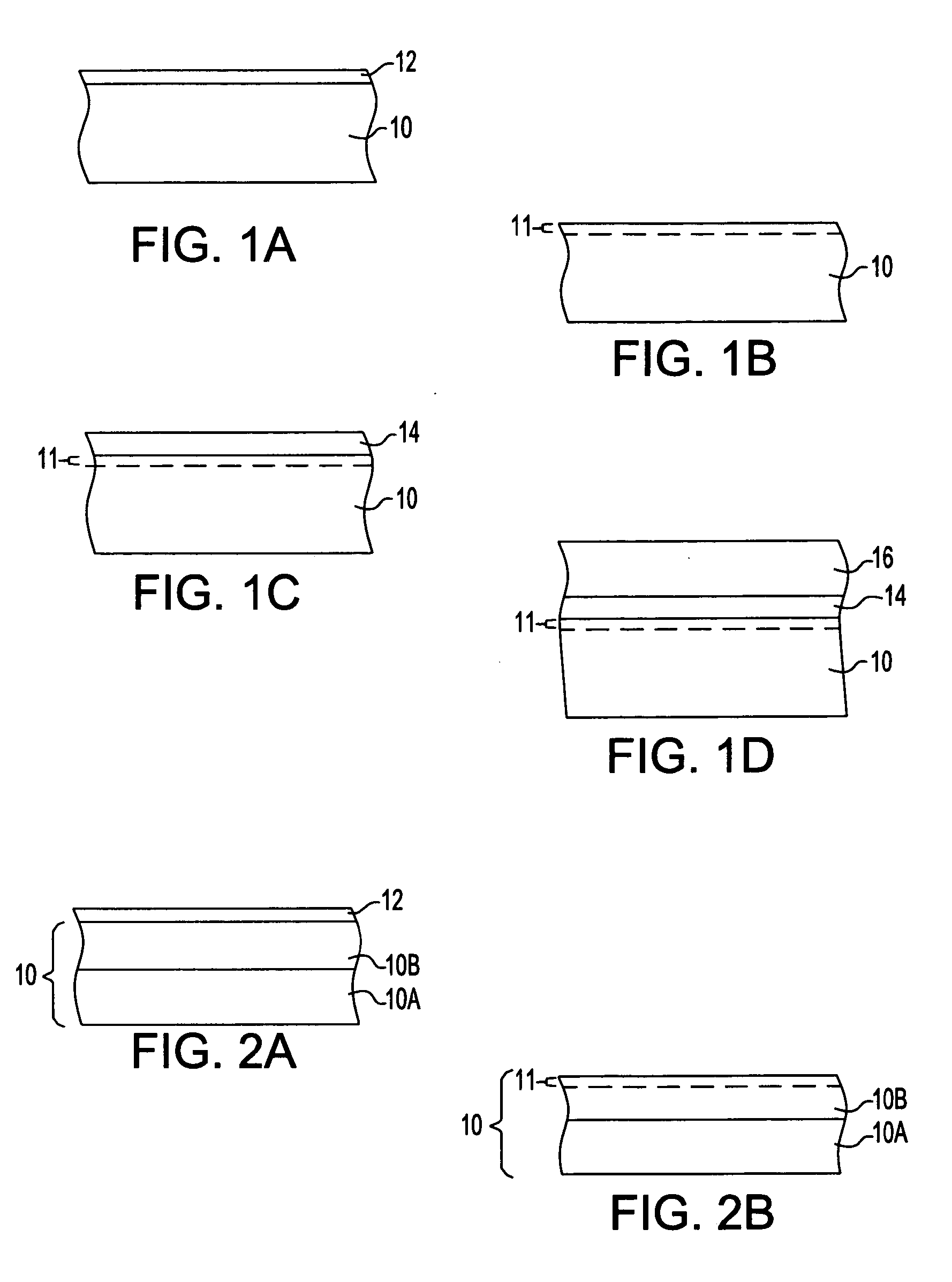
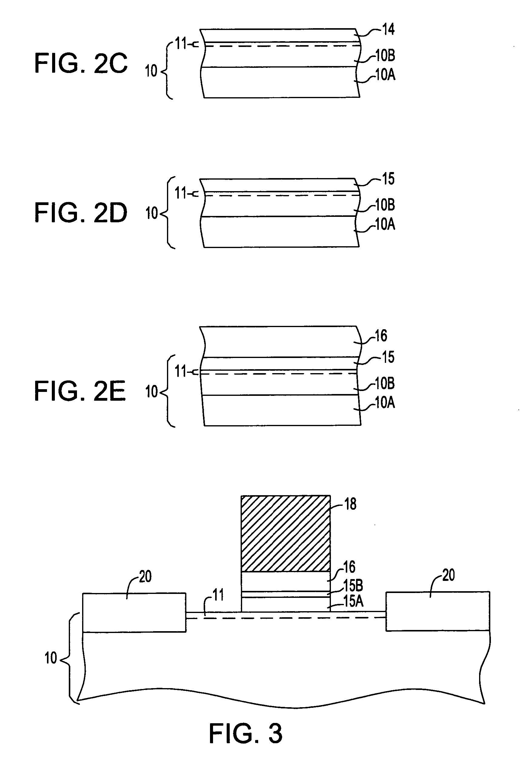
[0081]In this example, a MOSCAP was prepared utilizing a semiconductor structure in accordance with the present invention. The inventive structure included, from bottom to top, an atomic-H passivated GaAs substrate, an amorphous Si layer, SiOx and HfO2. The structure was formed utilizing the inventive processing details described above. After formation, a gate electrode was formed thereon and the structure was annealed at 700° C., 1 min., in nitrogen.

[0082]FIG. 4A shows the CV curves of such a MOSCAP at 1 kHz, 10 kHz, 100 kHz and 1 MHz. Specifically, the CV curves have very low frequency dispersion, which is indicative of low interface state density. FIG. 4B shows the Dit extracted as a function of gate voltage of the same MOSCAP as in FIG. 4A using the frequency-dependent method well known in the art. The results show a minimum Dit value of 6×1011 cm−2 / eV, which is over an order of magnitude lower than typically obtained on MOSCAPs with HfO2 directly on an unpassivated GaAs.


PUM

PropertyMeasurementUnit
temperatureaaaaaaaaaa
temperaturesaaaaaaaaaa

Abstract

A method of forming a high k gate stack on a surface of a III-V compound semiconductor, such GaAs, is provided. The method includes subjecting a III-V compound semiconductor material to a precleaning process which removes native oxides from a surface of the III-V compound semiconductor material; forming a semiconductor, e.g., amorphous Si, layer in-situ on the cleaned surface of the III-V compound semiconductor material; and forming a dielectric material having a dielectric constant that is greater than silicon dioxide on the semiconducting layer. In some embodiments, the semiconducting layer is partially or completely converted into a layer including at least a surface layer that is comprised of AOxNy prior to forming the dielectric material. In accordance with the present invention, A is a semiconducting material, preferably Si, x is 0 to 1, y is 0 to 1 and x and y are both not zero.

Description

CROSS REFERENCE TO RELATED APPLICATION[0001]This application is a divisional of U.S. patent application Ser. No. 11 / 327,675, filed Jan. 6, 2006 the entire content and disclosure of which is incorporated herein by reference.DESCRIPTION[0002]1. Field of the Invention[0003]The present invention relates to a semiconductor structure, and more particularly to a semiconductor structure including a dielectric material having a dielectric constant of greater than that of silicon dioxide located on a passivated surface of a III-V compound semiconductor in which the passivated surface has electrical properties that are sufficient for high-performance field effect transistor (FET) applications. The present invention also provides a method of fabricating such a semiconductor structure.[0004]2. Background of the Invention[0005]In semiconductor technology, an elemental semiconductor material such as, for example, Si or Ge, is typically used as a substrate in which one or more semiconductor devices...

Claims


Application Information

Patent Timeline
Patent Type & Authority Applications(United States)
IPC IPC(8): H01L29/267H01L21/20H01L21/336H01L21/324
CPCH01L21/28158H01L21/3145H01L21/31645H01L29/513H01L29/518H01L2924/0002H01L29/78H01L2924/00H01L21/02271H01L21/02148H01L21/02181H01L21/3205H01L21/32051
Inventor FOMPEYRINE, JEANKIEWRA, EDWARD W.KOESTER, STEVEN J.SADANA, DEVENDRA K.WEBB, DAVID J.
Owner GLOBALFOUNDRIES U S INC
Why Eureka
Try Eureka