Image sensor having improved sensitivity and decreased crosstalk and method of fabricating same

a technology of image sensor and crosstalk, which is applied in the field of image sensor, can solve the problems of reducing the sensitivity of the mos image sensor, crosstalk between adjacent pixels, and reducing the separation of active devices, so as to achieve the effect of reducing crosstalk and improving sensitivity

Active Publication Date: 2007-08-23
SAMSUNG ELECTRONICS CO LTD
View PDF1 Cites 119 Cited by
  • Summary
  • Abstract
  • Description
  • Claims
  • Application Information

AI Technical Summary

Benefits of technology

[0013]Accordingly, embodiments of the present invention have been made keeping in mind at least the above problems and such embodiments provide an image sensor having improved sensitivity and decreased crosstalk. Embodiments of the invention also provide a method of fabricating such an image sensor.

Problems solved by technology

Unfortunately, reduction in the physical size of the photoelectric transducer device results in a corresponding reduction in the sensitivity of the MOS image sensor.
This decrease in active device separation leads to crosstalk between adjacent pixels.
This phenomenon is particularly prevalent where the inter-layer dielectric films have non-uniform surfaces.
When crosstalk occurs, the resolution is degraded in the case of a gray image sensor to the point where the resulting image is distorted.
However, there is a limitation to the depth at which p-type doping regions 3b may be formed under STI region 3a.
Thus, it is not possible to satisfactorily provide an electrical crosstalk barrier.
Furthermore, the p-type doping region 3b does not provide an effective optical crosstalk barrier.

Method used


Image

  • Image sensor having improved sensitivity and decreased crosstalk and method of fabricating same
  • Image sensor having improved sensitivity and decreased crosstalk and method of fabricating same
  • Image sensor having improved sensitivity and decreased crosstalk and method of fabricating same

Examples


Embodiment Construction

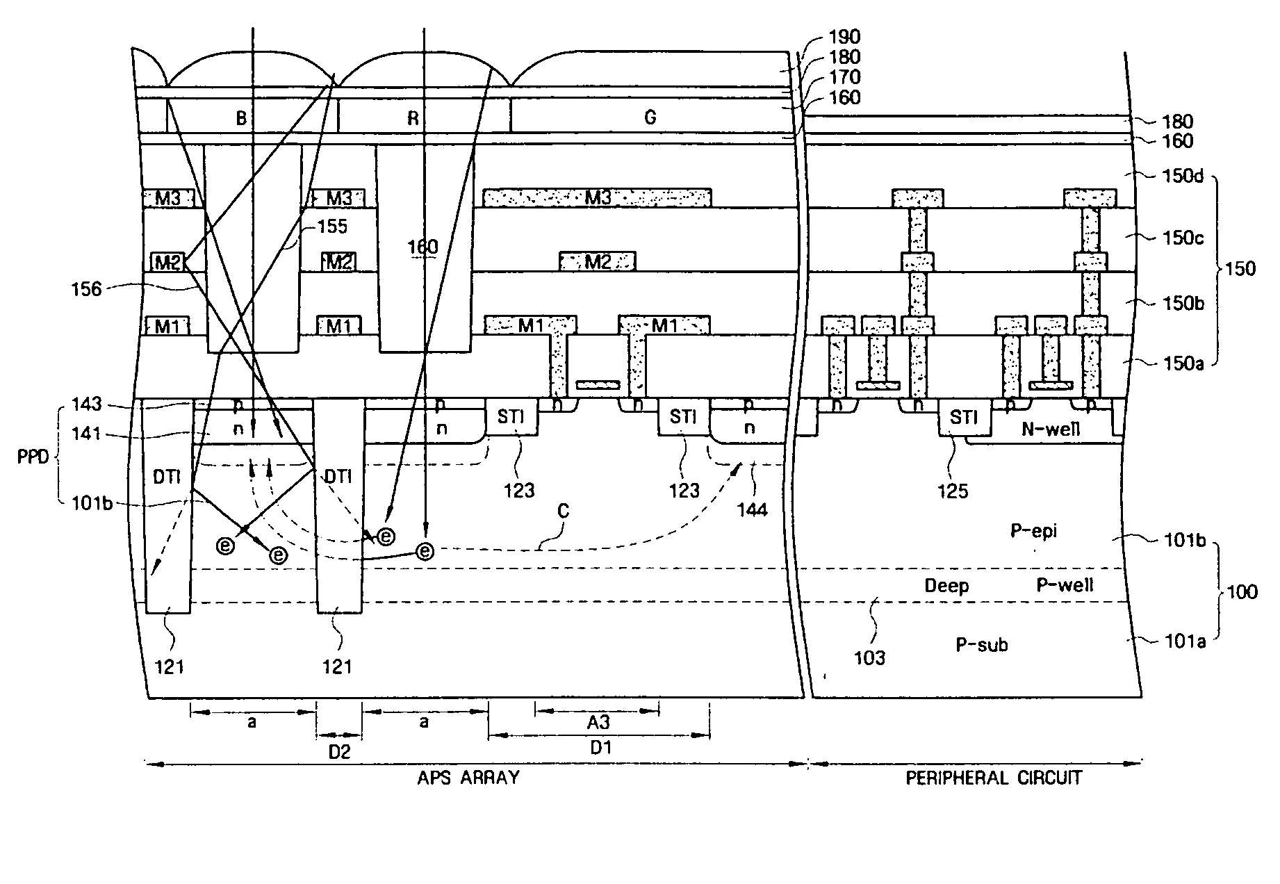
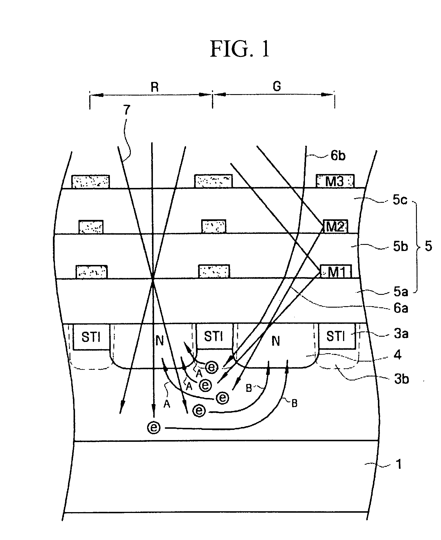
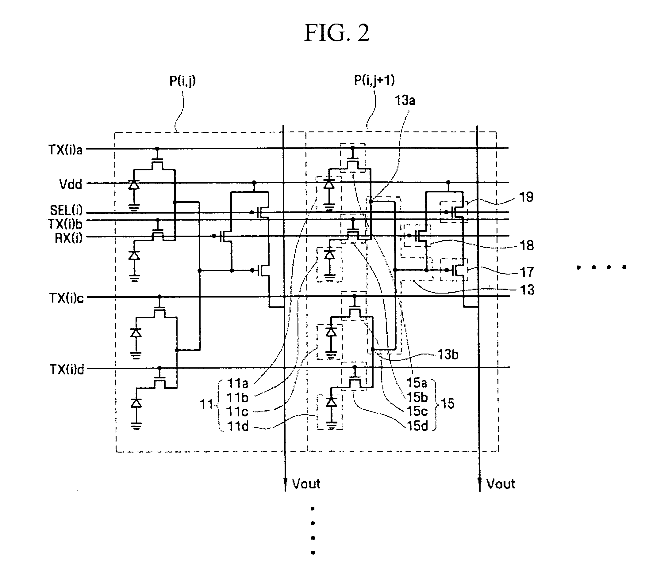
[0034]Merits and characteristics of the invention, and methods for accomplishing them will become more apparent from the following embodiments taken in conjunction with the accompanying drawings. However, the present invention is not limited to the disclosed embodiments, but may be implemented in various manners. The embodiments are provided to complete the disclosure of the present invention and to allow those having ordinary skill in the art to understand the scope of the present invention. The present invention is defined by the category of the claims. In some embodiments, well-known processes, well-known device structures and well-known technologies will not be described in detail to avoid obscuring the present invention.

[0035]The same reference numerals in different drawings denote the same or similar elements. As used herein, the term “and / or” includes any and all combinations of one or more of the associated listed items. It is emphasized that the term “comprises” or “compris...


PUM


Abstract

An image sensor is provided. The image sensor includes a substrate; a first isolation region, a second isolation region, a plurality of photoelectric transducer devices, a read element and a floating diffusion region. The second isolation region has a depth that is less than that of the first isolation region. The plurality of photoelectric transducer devices is isolated from one another by the first isolation region. The read element and the floating diffusion region are isolated from the photoelectric transducer devices by the second isolation region.

Description

BACKGROUND OF THE INVENTION[0001]1. Field of the Invention[0002]The present invention relates to an image sensor. More particularly, the invention relates to an image sensor having improved sensitivity and decreased crosstalk, as well as a method of fabricating such an image sensor.[0003]This application claims priority from Korean Patent Application No. 10-2006-0009372 filed on Jan. 31, 2006, the subject matter of which is hereby incorporated by reference in its entirety.[0004]2. Description of the Related Art[0005]An image sensor converts optical images into electrical signals. Recent evolution in various consumer products (e.g., digital cameras, camcorders, Personal Communication Systems (PCSs), game equipment, surveillance cameras and medical micro-cameras) has resulted in a sharp increase in the demand for image sensors having improved performance characteristics.[0006]Conventionally, Metal Oxide Semiconductor (MOS) image sensors have been used within a variety of optical imagi...

Claims


Application Information

Patent Timeline
Patent Type & Authority Applications(United States)
IPC IPC(8): H01L31/113H01L31/062
CPCH01L27/14625H01L27/1463H01L27/14629H01L27/146
Inventor MOON, CHANG-ROKLEE, YUN-HEEJUNG, JONG-WANPARK, BYUNG-JUN
Owner SAMSUNG ELECTRONICS CO LTD
Why Eureka
Try Eureka