Method of manufacturing light emitting diode package

a technology of light-emitting diodes and manufacturing methods, which is applied in the direction of discharge tubes/lamp details, discharge tubes luminescnet screens, filing appliances, etc., can solve the problems of low light extraction efficiency and low light extraction efficiency

Active Publication Date: 2007-08-23
SAMSUNG ELECTRONICS CO LTD
View PDF7 Cites 26 Cited by
  • Summary
  • Abstract
  • Description
  • Claims
  • Application Information

AI Technical Summary

Benefits of technology

[0012]The present invention has been made to solve the foregoing problems of the prior art and therefore an aspect of the present invention is to provide a method of ma

Problems solved by technology

This results in low light extraction efficiency.
In addition, as shown in FIG. 1, when a liquid transparent resin is injected through a dispensing procedure, etc. to form the resin encapsulant 16 in the r

Method used


Image

  • Method of manufacturing light emitting diode package
  • Method of manufacturing light emitting diode package
  • Method of manufacturing light emitting diode package

Examples


Embodiment Construction

[0031]Exemplary embodiments of the present invention will now be described in detail with reference to the accompanying drawings.

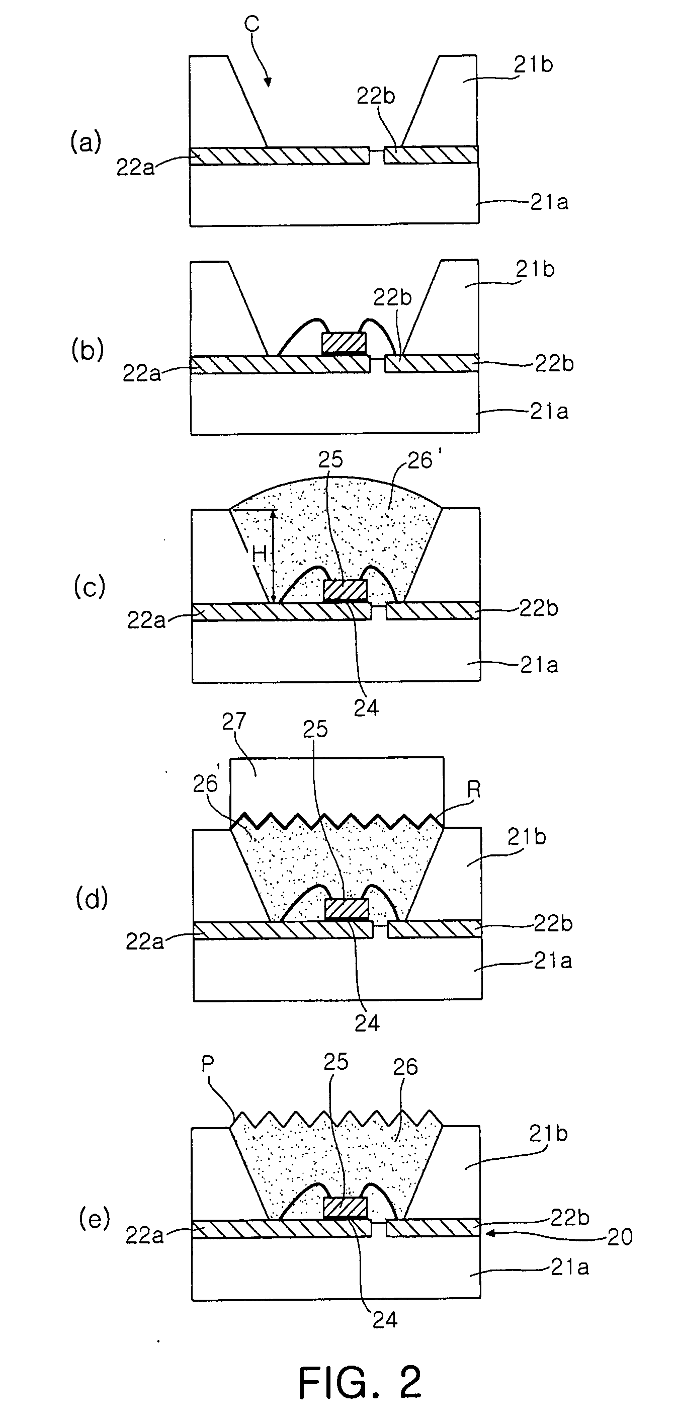
[0032]FIG. 2(a) to 2(e) are sectional views illustrating a method of manufacturing a light emitting diode package according to the present invention.

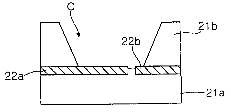
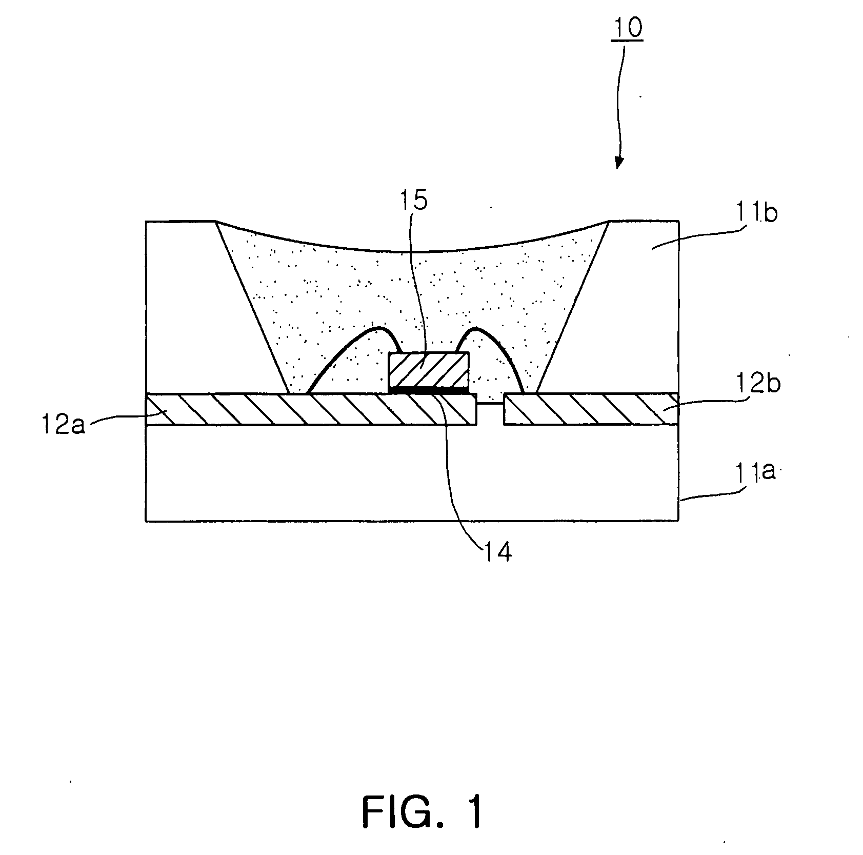
[0033]First, as shown in FIG. 2(a), a cup-shaped structure 21 having a recess C and electrode patterns 22a and 22b formed at least on a bottom of the recess C is provided. The inner sidewall of the recess C can be used as an upwardly-inclined reflecting surface. The package structure 21 adopted in this embodiment exemplifies one that is composed of a lower substrate 21a having the electrode patterns 22a and 22b and an upper substrate 21b having a recess, which however does not limit the present invention. The package substrate 21 can be any other package substrate having a cup structure for mounting a chip therein. In addition, the electrode patterns 22a and 22b can be understood as an electrode structure conn...


PUM


Abstract

A method of manufacturing a light emitting diode package. A cup-shaped package structure with a recess formed therein and an electrode structure formed on a bottom of the recess is prepared. A light emitting diode chip is mounted on a bottom of the recess with a terminal of the chip electrically connected to the electrode structure. A liquid-state transparent resin is injected in the recess and before the liquid-state transparent resin is completely cured, a stamp with a micro rough pattern engraved thereon is applied on an upper surface of the resin. The liquid-state transparent resin is cured with the stamp applied thereon to form a resin encapsulant and the stamp is removed from the resin encapsulant.

Description

CLAIM OF PRIORITY[0001]This application claims the benefit of Korean Patent Application No. 2006-0017390 filed on Feb. 22, 2006, in the Korean Intellectual Property Office, the disclosure of which is incorporated herein by reference.BACKGROUND OF THE INVENTION[0002]1. Field of the Invention[0003]The present invention relates to a method of manufacturing a light emitting diode package and, more particularly, to a method of manufacturing a light emitting diode package which forms a micro structure for improving light extraction efficiency of a light emitting diode.[0004]2. Description of the Related Art[0005]A light emitting diode is a semiconductor device for converting electric energy to light energy and is composed of a compound semiconductor that generates a particular wavelength of light according to an energy band gap. Recently, light emitting diodes are utilized in various applications such as optical communication, display and the like.[0006]Light emitting diodes are provided ...

Claims


Application Information

Patent Timeline
IPC IPC(8): H01L21/00H01L33/50H01L33/22H01L33/54H01L33/56H01L33/62
CPCH01L33/54H01L2224/32225H01L2224/48091H01L2224/48247H01L2224/73265H01L2924/00014B42F21/02B42B5/08
Inventor PARK, YOUN GONLEE, JONG MYEONLEE, HAI SUNGCHANG, MYUNG WHUNCHOO, HO SUNG
Owner SAMSUNG ELECTRONICS CO LTD
Why Eureka
Try Eureka