
Semiconductor arrangement and method for operating a semiconductor arrangement

Inactive Publication Date: 2007-08-23
QIMONDA
View PDF9 Cites 4 Cited by
  • Summary
  • Abstract
  • Description
  • Claims
  • Application Information

AI Technical Summary

Benefits of technology

[0012] In one aspect, the present invention provides a semiconductor arrangement and also a method for operating a semiconductor arrangement in which the problems described above are avoided and the reliability of the semiconductor arrangement is increased.

Problems solved by technology

Memory modules which are arranged far away with respect to the memory controller have a high latency.
Since the memory device only has one interface between the memory controller and the memory modules, moreover, the bandwidth for the data transfer is limited.
This leads to a high power consumption of the semiconductor arrangement.

Method used


Image

  • Semiconductor arrangement and method for operating a semiconductor arrangement
  • Semiconductor arrangement and method for operating a semiconductor arrangement
  • Semiconductor arrangement and method for operating a semiconductor arrangement

Examples


Embodiment Construction

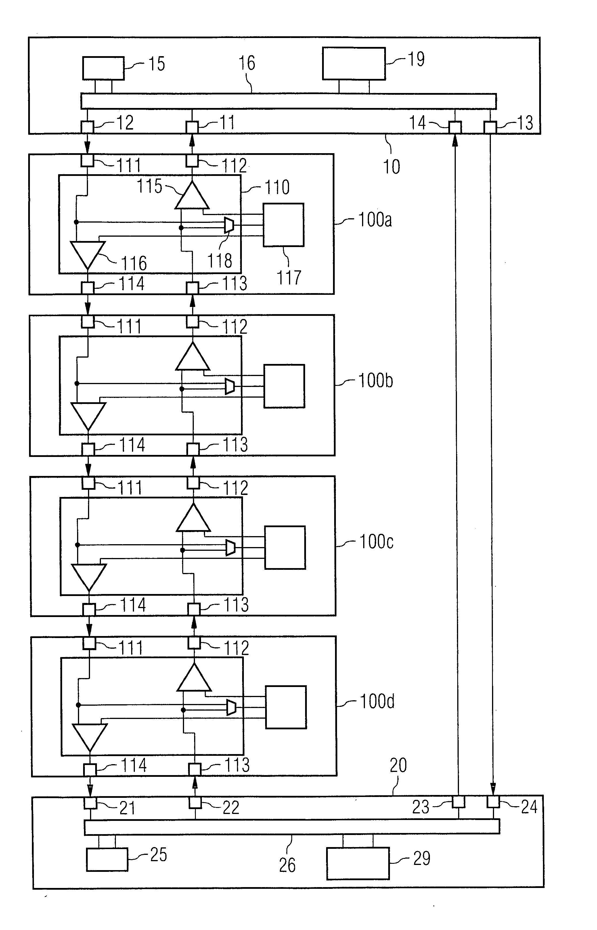
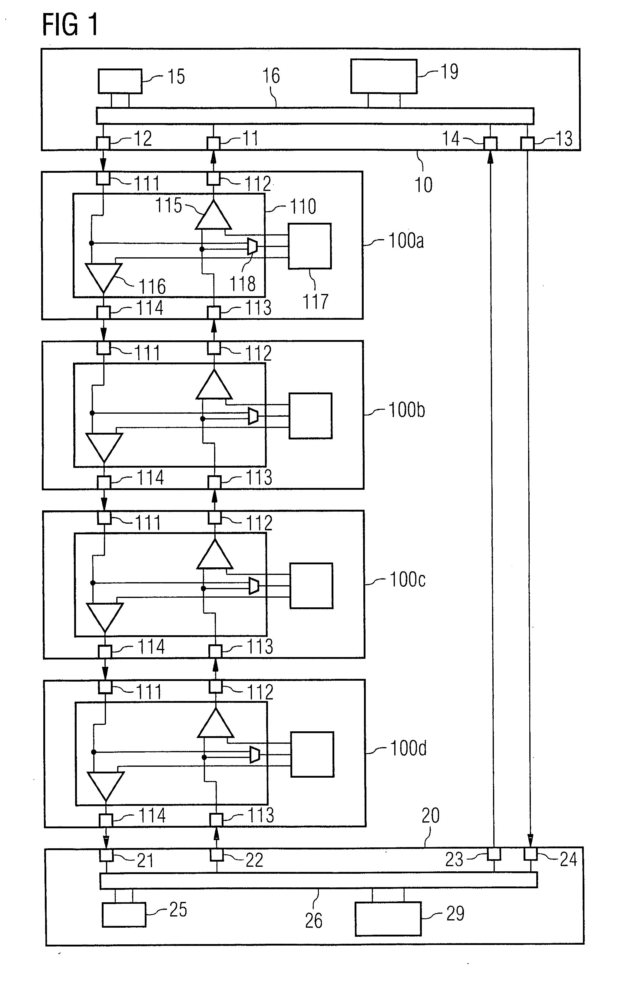
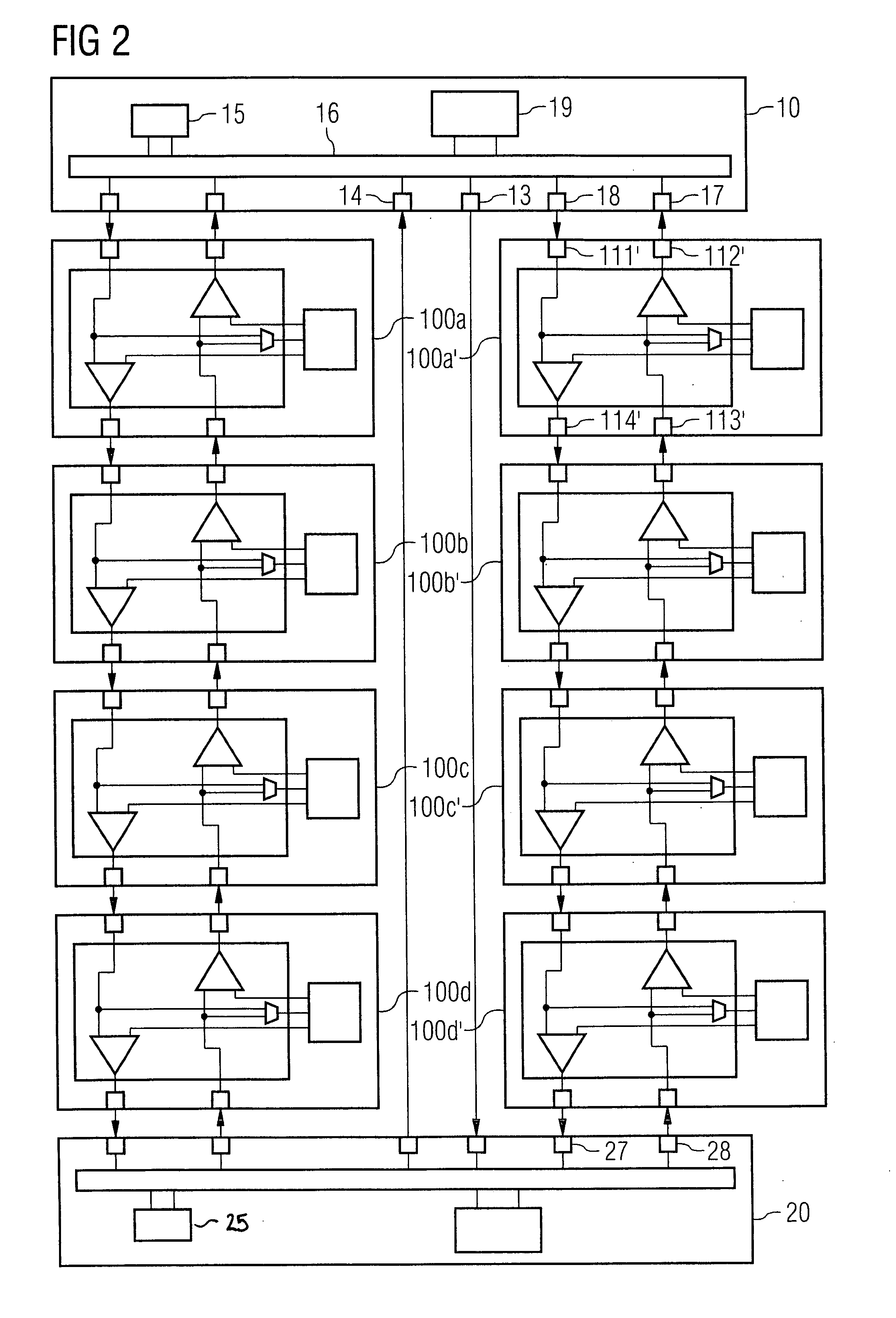
[0024]FIG. 1 shows a schematic illustration of a semiconductor arrangement in accordance with one embodiment of the invention. The semiconductor arrangement comprises a first control unit 10, second control unit 20 and also a multiplicity of memory modules 100a, 100b, 100c and 100d which are arranged in a chain. The first control unit 10 and the second control unit 20 are in each case arranged at remote ends of the chain of memory modules 100a, 100b, 100c and 100d. The memory modules 100a, 100b, 100c and 100d are embodied identically.

[0025] A first direction as used herein relates to a direction along a ring-shaped conductive path proceeding from the first control unit 10 towards a first one 100a of the memory modules, coupling the memory modules in series, proceeding from a last one 100d of the memory modules towards the second control unit 20 and proceeding from the second control unit 20 to the first control unit 10.

[0026] A second direction as used herein relates to a directio...


PUM


Abstract

A semiconductor arrangement includes a first control unit, a second control unit and at least one memory module. Between the first control unit and the at least one memory module and between the second control unit and the at least one memory module, data can be transferred both in a first direction and in a second direction. The at least one memory module includes a first input interface for receiving data from a first direction, a first output interface for transmitting data in a second direction, a second input interface for receiving data from the second direction, and a second output interface for transmitting data in the first direction. In order to transmit and receive data in the first and second direction, respectively, in each case first and second input interfaces and in each case first and second output interfaces are provided in the case of the first and in the case of the second control unit. The second output interface of the first control unit is coupled to the second input interface of the second control unit, and the second output interface of the second control unit is coupled to the second input interface of the first control unit.

Description

[0001] This application claims priority to German Patent Application 10 2006 006 571.9, which was filed Feb. 13, 2006, and is incorporated herein by reference. TECHNICAL FIELD [0002] The present invention relates to a semiconductor arrangement and to a method for operating a semiconductor arrangement. The invention relates in particular to semiconductor arrangements comprising a plurality of control units and a multiplicity of memory modules. BACKGROUND [0003] For data storage, computer systems usually have a memory controller and memory devices such as, for instance, read / write memories or random access memories (RAM memories) which are embodied for example as FB-DIMM (Fully Buffered Dual Inline Memory Module). Each of the FB-DIMMs comprises a memory component for storing data, a memory interface and an advanced memory buffer (AMB). The AMB serves to control the data interchange between the memory controller and the memory component. AMB receives write or command data in serial for...

Claims


Application Information

Patent Timeline
IPC IPC(8): G06F12/00
CPCG11C5/04
Inventor RISSE, GERHARD
Owner QIMONDA
Learn More