Method and system for improving yield of an integrated circuit

a technology of integrated circuits and yields, applied in the field of electronic design automation tools, can solve problems such as insufficient increase of methods, and mismatch effects of simple “fast” devices and “slow” devices, and achieve the effect of improving the yield of integrated circuits

Active Publication Date: 2007-08-23
CADENCE DESIGN SYST INC
View PDF5 Cites 27 Cited by
  • Summary
  • Abstract
  • Description
  • Claims
  • Application Information

AI Technical Summary

Benefits of technology

[0014]FIG. 2 illustrates a method of improving yield of an integrate

Problems solved by technology

This is because the variation of device property, especially mismatch effects, increases as the device size shrinks to submicron processing technology.
This method is limited for the following reasons.
First, unlike most digital circuits, the typical analog circuit has many varied performance specifications and requires a richer set of simulations to qualify.
The simple “fast” device and “slow” device worst-case corner methods are not adequate for analog circuits.
Thus, simulating worst-case corners can quickly become infeasible in determining mismatch effects.
Furthermore, the worst-case corner method does not typically consider the distribution of parameters and the correlation information between the parameters.
Consequently, an integrated circuit designed using this method often turns out to

Method used


Image

  • Method and system for improving yield of an integrated circuit
  • Method and system for improving yield of an integrated circuit
  • Method and system for improving yield of an integrated circuit

Examples


Embodiment Construction

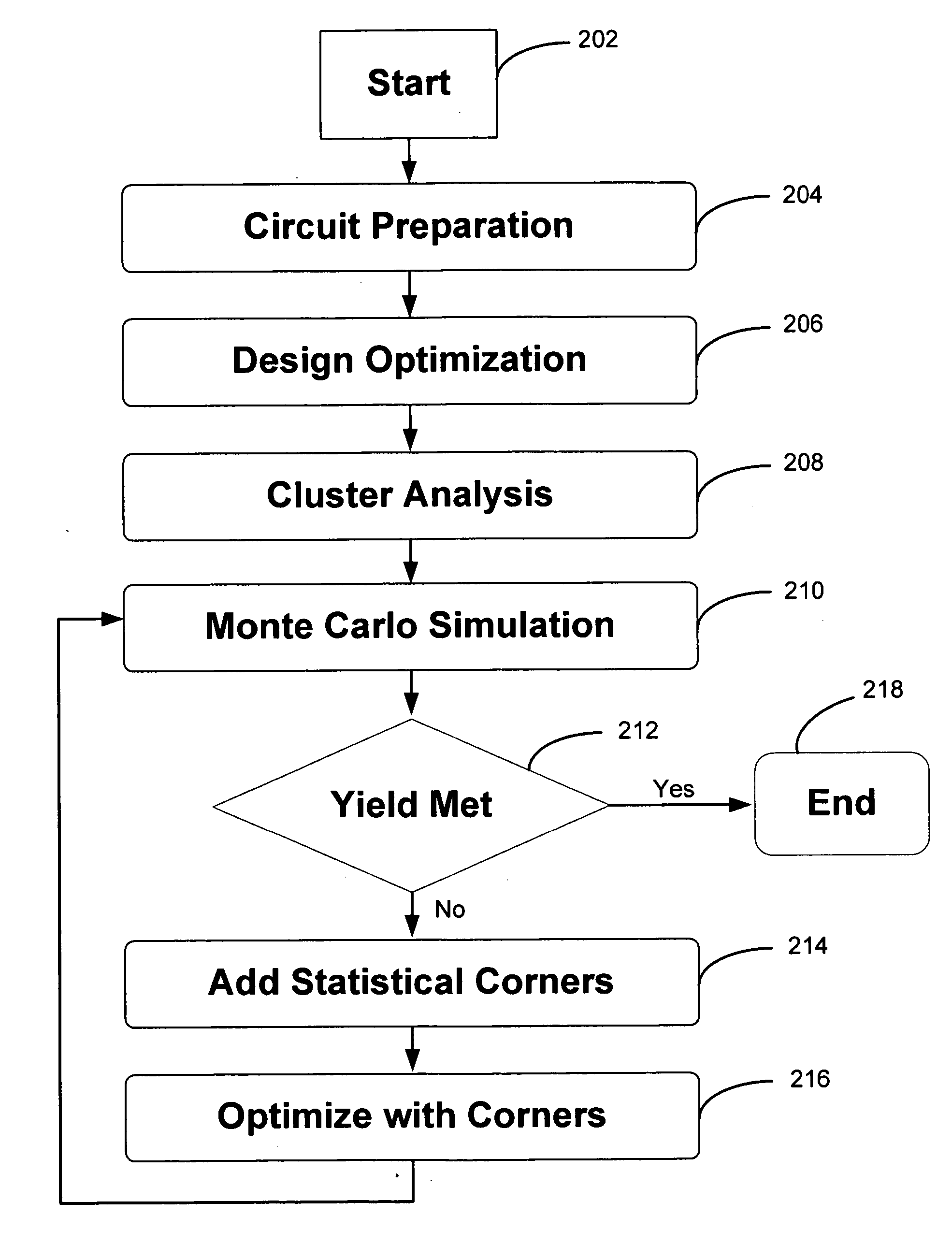
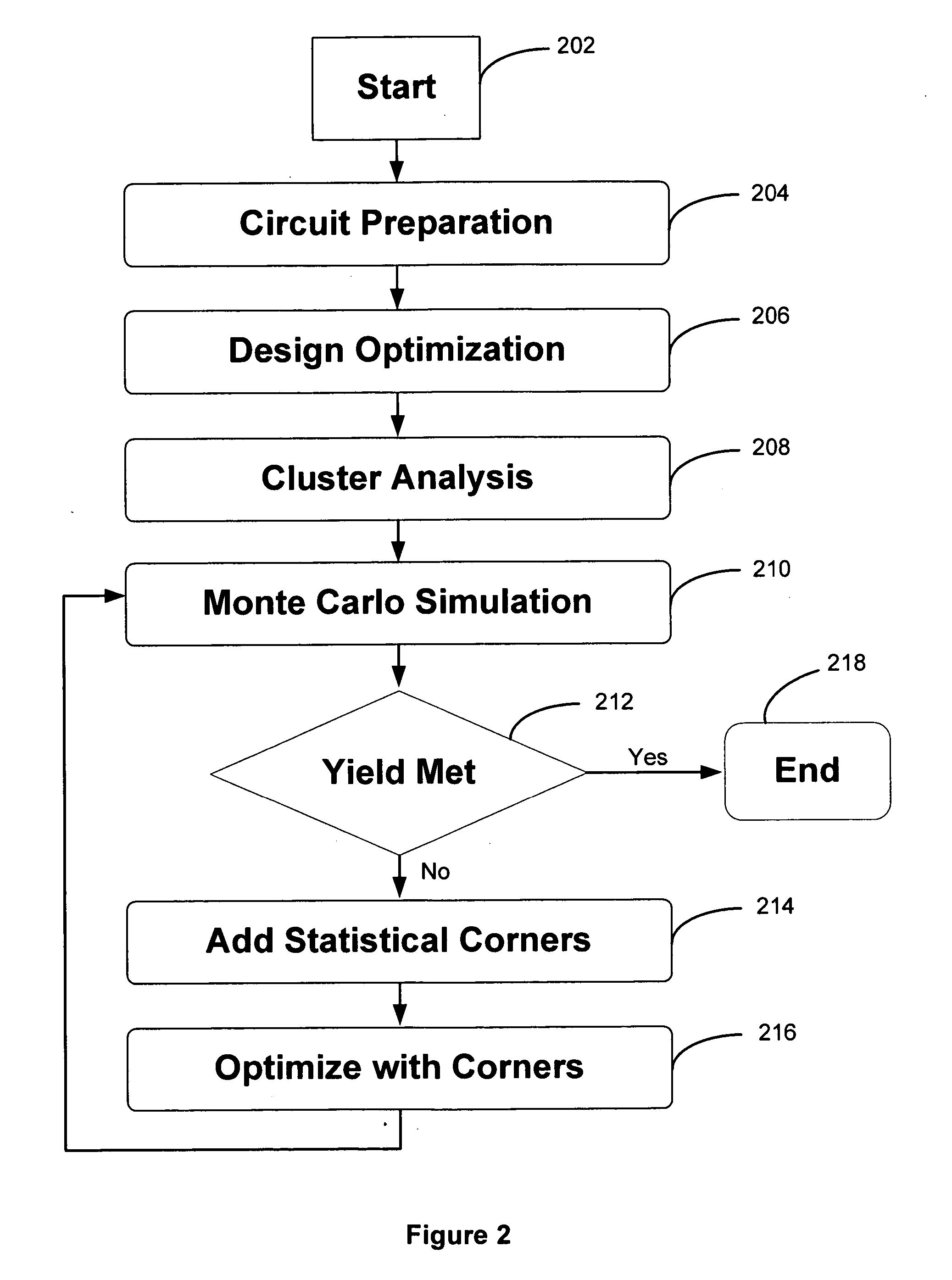
[0022] Methods and systems are provided for improving yield of an integrated circuit. The following descriptions are presented to enable any person skilled in the art to make and use the invention. Descriptions of specific embodiments and applications are provided only as examples. Various modifications and combinations of the examples described herein will be readily apparent to those skilled in the art, and the general principles defined herein may be applied to other examples and applications without departing from the spirit and scope of the invention. Thus, the present invention is not intended to be limited to the examples described and shown, but is to be accorded the widest scope consistent with the principles and features disclosed herein.

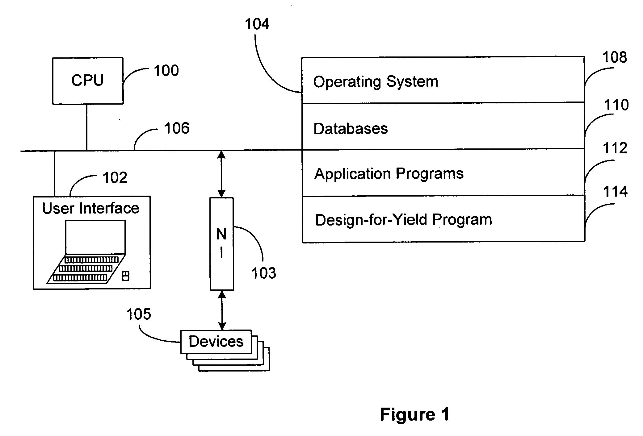
[0023] In one embodiment, a circuit optimizer is implemented using a computer system schematically shown in FIG. 1. The computer system includes one or more central processing units (CPUs) 100, at least a user interface 102, a memory devi...


PUM


Abstract

Method and system for improving yield of an integrated circuit are disclosed. The method includes optimizing a design of the integrated circuit according to a set of predefined design parameters to generating design points that meet a set of predefined design specifications, analyzing the design points to form clusters comprising the design points, determining a representative design point from the clusters comprising the design points, running a statistical simulation to determine a yield of the design using the representative design point and a statistical model of manufacturing process variations, generating statistical corners in accordance with results of the statistical simulation, and optimizing the design in accordance with the statistical corners using an iterative process.

Description

FIELD OF THE INVENTION [0001] The present invention relates to the field of electronic design automation tools. In particular, the present invention relates to a method and system for improving yield of an integrated circuit. BACKGROUND OF THE INVENTION [0002] The yield of an integrated circuit is directly related to the profitability of a product, and that increasing yield by even a few percentage points may save a company millions of dollars. It is well known that integrated circuit manufacturing processes have inherent variations that cause the performance of a design to vary from one chip to another. A product's yield is the percentage of manufactured designs that pass all performance specifications. [0003] The yield of an integrated circuit is the ratio of the number of chips that meets specifications in certain conditions to the total number of chips that are manufactured. There are two types of yield. One type is referred to as the functional field, which measures percentage ...

Claims


Application Information

Patent Timeline
IPC IPC(8): G06F17/50
CPCG06F17/5068G06F17/5036G06F30/367G06F30/39
Inventor LIU, HONGZHOUPHELPS, RODNEY M.
Owner CADENCE DESIGN SYST INC
Why Eureka
Try Eureka