This helps you quickly interpret patents by identifying the three key elements:
Problems solved by technology
Method used
Benefits of technology
Benefits of technology
[0013] Through research for solving the foregoing subject, the inventors found that organic EL devices can emit light in different colors (multicolor emission) by adjusting optical thickness of a resonator in each device formed on the same substrate using an inorganic compound layer, and that an organic luminescent medium layer, light reflective layer, transparent electrode and the like can be each formed as a single common layer even in organic EL devices (pixels) emitting light in different colors without need of forming different layers in each device so that an organic EL display with high efficiency can easily fabricated. They completed the invention based on the findings.
[0023] The organic EL display according to the invention allows multicolor emission without decreasing the luminous efficiency of the organic EL device by forming the organic EL devices having different resonators on a substrate.
[0024] Since the optical thickness of the optical resonator is controlled by forming the inorganic compound layer over the light reflective conductive layer, the optical thickness of each organic EL device part can be arbitrarily adjusted without changing the thickness of the organic luminescent medium layer optimally set for the emitting device.
[0025] Moreover, since the thickness of the organic luminescent medium layer and the like need not be adjusted in units of EL device parts which emit light of different colors, the organic EL display according to the invention can be easily produced.BRIEF DESCRIPTION OF THE DRAWINGS
Problems solved by technology
On the other hand, since it is difficult to realize a high-definition display using the three-color pattern formation method due to difficulty in forming a three-color pattern, it is considered that a large-screen display cannot be formed.
The method of combining white EL with a color filter has a problem in which white EL emission efficiency is poor.
The method of combining EL with a color conversion film has a problem such as a poor red conversion efficiency, although various improvements have been made.
However, the above EL device or display has the following problems.
This requires that the EL device have a thickness corresponding to each color in pixel units, thereby making production difficult.
(2) The light selectivity may be insufficient since conditions where m in the above expression is small are utilized.
Method used
Image
Click on the blue label to locate the original text in one second.
Reading with bidirectional positioning of images and text.
Examples
first embodiment
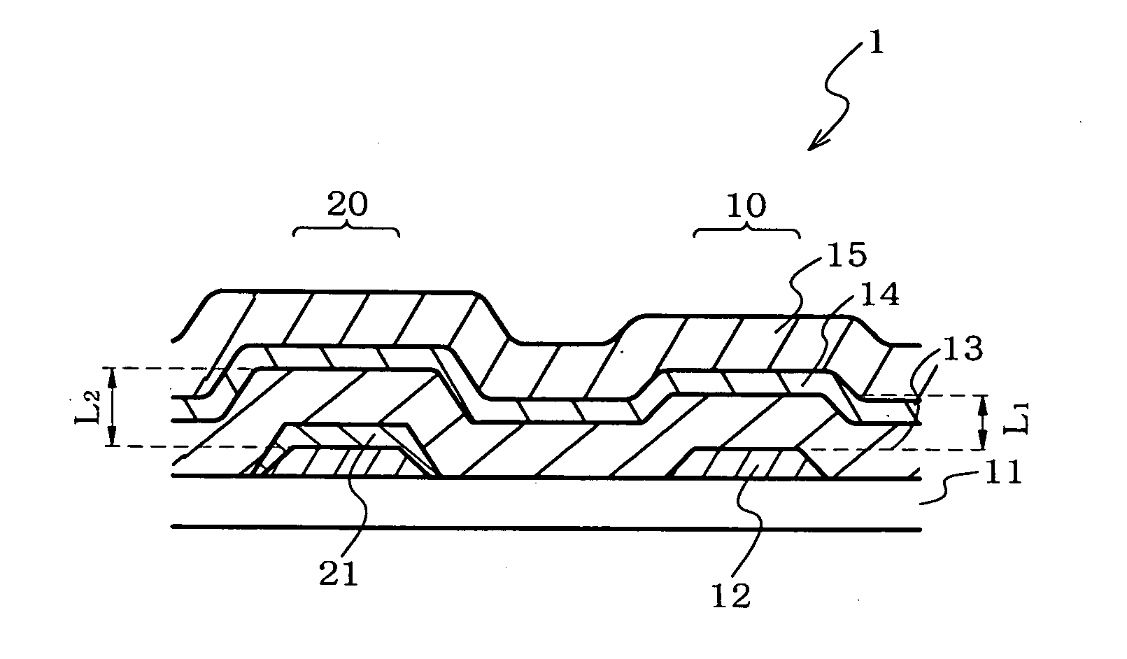
[0033]FIG. 1 is a view showing an organic EL display according to a first embodiment of the invention.
[0034] An organic EL display 1 includes a first organic EL device part 10 and a second organic EL device part 20 placed side by side on a substrate 11.
[0035] The first organic EL device part 10 has a structure in which a light reflective conductive layer 12, an organic luminescent medium layer 13, a light reflective layer 14, and a transparent electrode layer 15 are stacked in this order on the substrate 11.
[0036] The second organic EL device part 20 has a structure in which the light reflective conductive layer 12, a first inorganic compound layer 21, the organic luminescent medium layer 13, the light reflective layer 14, and the transparent electrode layer 15 are stacked in this order on the substrate 11.
[0037] The light reflective conductive layer 12 functions as an electrode which supplies holes or electrons, and reflects light from the organic luminescent medium layer 13 in...
second embodiment
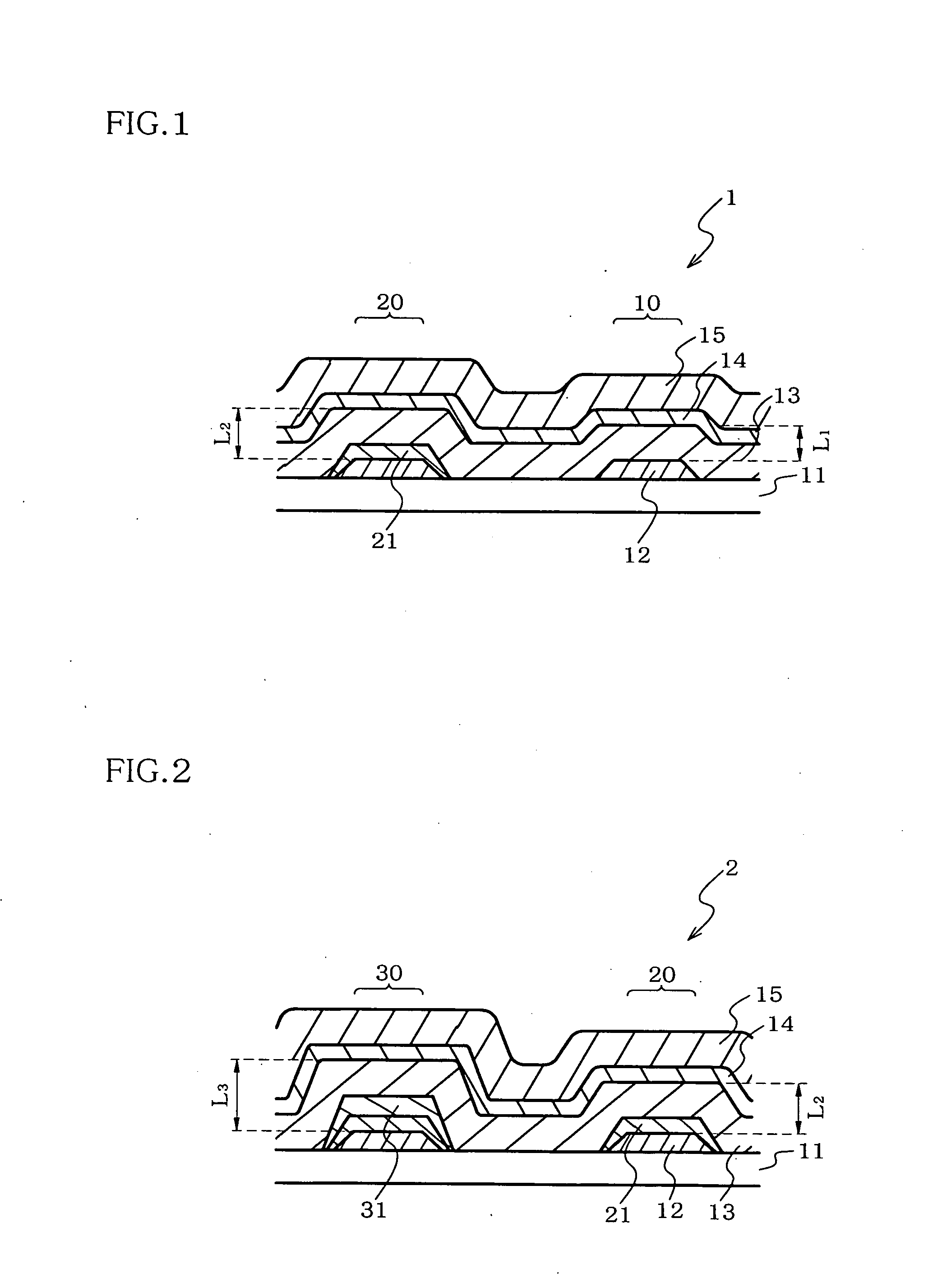
[0044]FIG. 2 is a view showing an organic EL display according to a second embodiment of the invention.
[0045] An organic EL display 2 includes the second organic EL device part 20 and a third organic EL device part 30 placed side by side on the substrate 11.
[0046] The second organic EL device part 20 is the same as in the first embodiment.
[0047] The third organic EL device part 30 has a structure in which the light-reflective conductive layer 12, the first inorganic compound layer 21, a second inorganic compound layer 31, the organic luminescent medium layer 13, the light-reflective layer 14, and the transparent electrode layer 15 are stacked in this order on the substrate 11. Specifically, the third organic EL device part 30 is formed in the same manner as the second organic EL device part 20 except that the second inorganic compound layer 31 is formed. The function of each layer is the same as in the second organic EL device part 20.
[0048] The second inorganic compound layer 3...
third embodiment
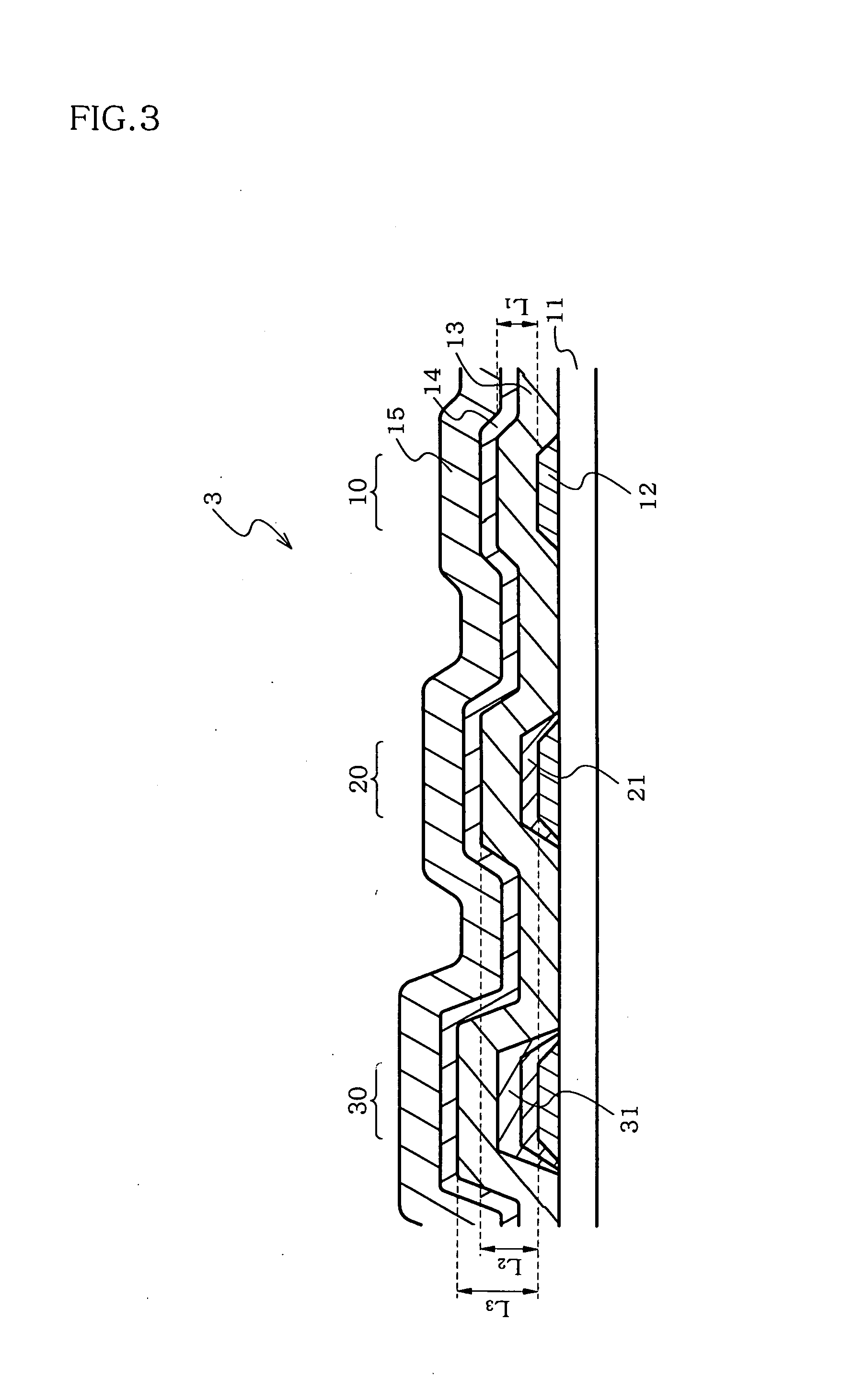
[0053]FIG. 3 is a view showing an organic EL display according to a third embodiment of the invention.
[0054] An organic EL display 3 includes the first organic EL device part 10, the second organic EL device part 20, and the third organic EL device part 30 placed side by side on the substrate 11.
[0055] The configuration of each of the organic EL device parts 10, 20, and 30 is the same as in the first and second embodiments. The function of each layer is also the same as in the first and second embodiments.
[0056] In the organic EL display 3, the organic EL device parts 10, 20, and 30 respectively have resonator structures which differ in the optical length (optical thickness). Specifically, the optical length is set at L1 for the first organic EL device part 10, set at L2 for the second organic EL device part 20, and set at L3 for the third organic EL device part 30.
[0057] Therefore, light having different wavelengths (λ1, λ, λ3) is respectively enhanced in the organic EL device ...
PUM
Abstract
An organic electroluminescent display (1) including: a substrate (11); and a first organic electroluminescent device part (10) and a second organic electroluminescent device part (20) placed side by side on a surface of the substrate; the first organic electroluminescent device part (10) including at least a light reflective conductive layer (12), an organic luminescent medium layer (13), and a transparent electrode layer (15) in this order and including a light reflective layer (14) inside or outside of the organic luminescent medium layer (13) or the transparent electrode layer (15); the second organic electroluminescent device part (20) including at least a light reflective conductive layer (12), a first inorganic compound layer (21), an organic luminescent medium layer (13), and a transparent electrode layer (15) in this order and including a light reflective layer (14) inside or outside of the organic luminescent medium layer (13) or the transparent electrode layer (15); and an emission spectrum of light from the first organic electroluminescent device part (10) differing from an emission spectrum of light from the second organic electroluminescent device part (20).
Description
TECHNICAL FIELD [0001] The invention relates to an organic electroluminescent display. In particular, the invention relates to an organic electroluminescent display in which multicolor emission is achieved by placing organic electroluminescent device parts provided with resonator structures having different optical lengths side by side on a substrate. BACKGROUND ART [0002] As technology of forming a full-color display using organic electroluminescence (“electroluminescence” and “electroluminescent” hereinafter may be abbreviated as “EL”), a three-color pattern formation method, a method of combining white EL with a color filter, a method of combining EL, a color conversion film, and a color filter, and the like have been known. [0003] The three-color pattern formation method may achieve a high efficiency by adjusting the material balance and reducing the loss of a circular polarizer. On the other hand, since it is difficult to realize a high-definition display using the three-color ...
Claims
Application Information
Patent Timeline
Application Date:The date an application was filed.
Publication Date:The date a patent or application was officially published.
First Publication Date:The earliest publication date of a patent with the same application number.
Issue Date:Publication date of the patent grant document.
PCT Entry Date:The Entry date of PCT National Phase.
Estimated Expiry Date:The statutory expiry date of a patent right according to the Patent Law, and it is the longest term of protection that the patent right can achieve without the termination of the patent right due to other reasons(Term extension factor has been taken into account ).
Invalid Date:Actual expiry date is based on effective date or publication date of legal transaction data of invalid patent.

