Memory array structure with strapping cells

Active Publication Date: 2007-08-30
TAIWAN SEMICON MFG CO LTD
View PDF14 Cites 37 Cited by
  • Summary
  • Abstract
  • Description
  • Claims
  • Application Information

AI Technical Summary

Benefits of technology

[0007] These and other problems are generally reduced, solved or circumvented, and technical advantages are genera

Problems solved by technology

One cause of this difference in the electrical and operational characteristics is the lithography process.
It has been found that this difference in density may affect some processes such as the etching rates and implantation concentration, thereby causing a difference in the electrical and operational characteristics between memory cells located near or along the edge (e.g., sparsely populated regions) and memory cells located in the inner regions of the memory array (e.g., densely populated regions).
Another cause is the well-proximity e

Method used


Image

  • Memory array structure with strapping cells
  • Memory array structure with strapping cells
  • Memory array structure with strapping cells

Examples


Embodiment Construction

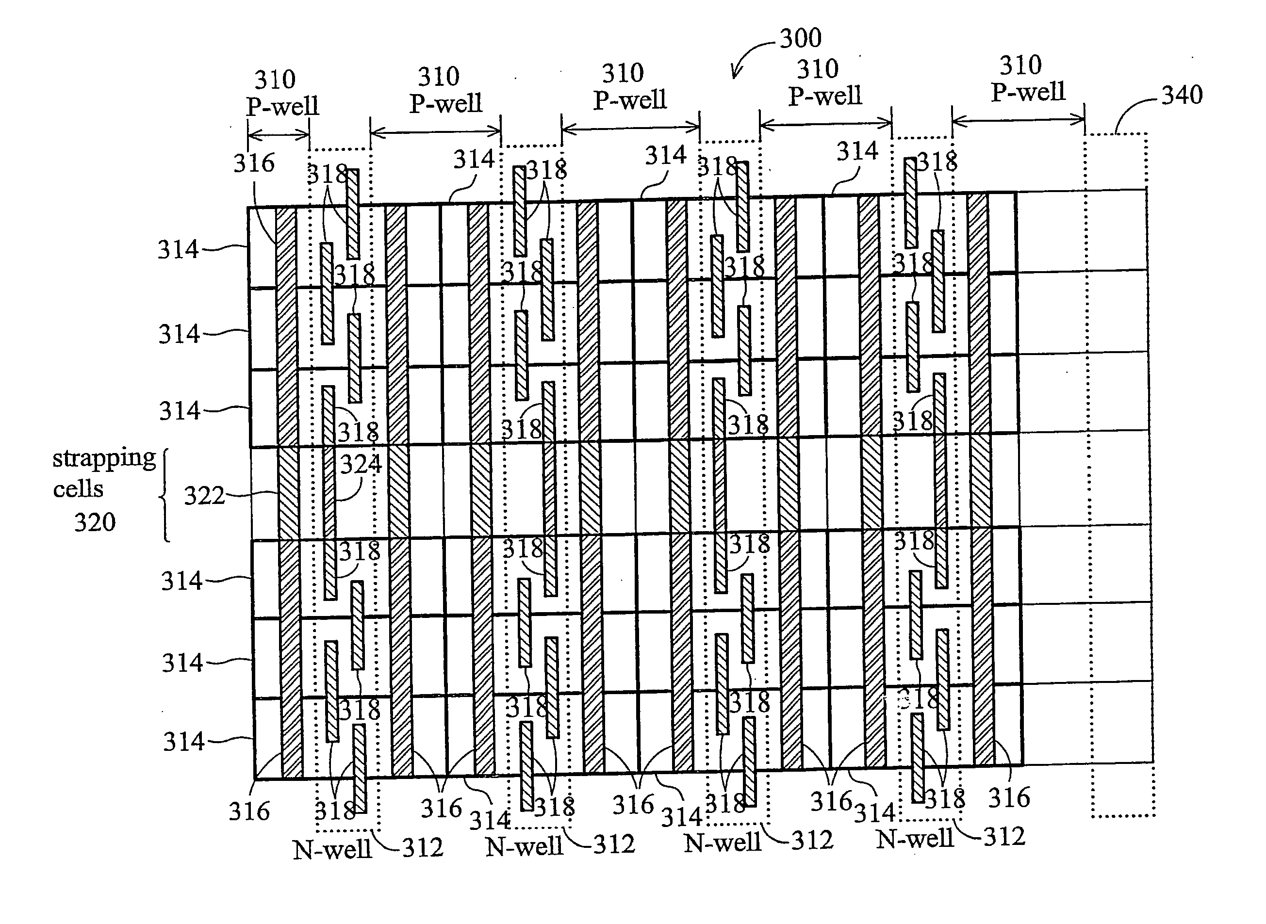
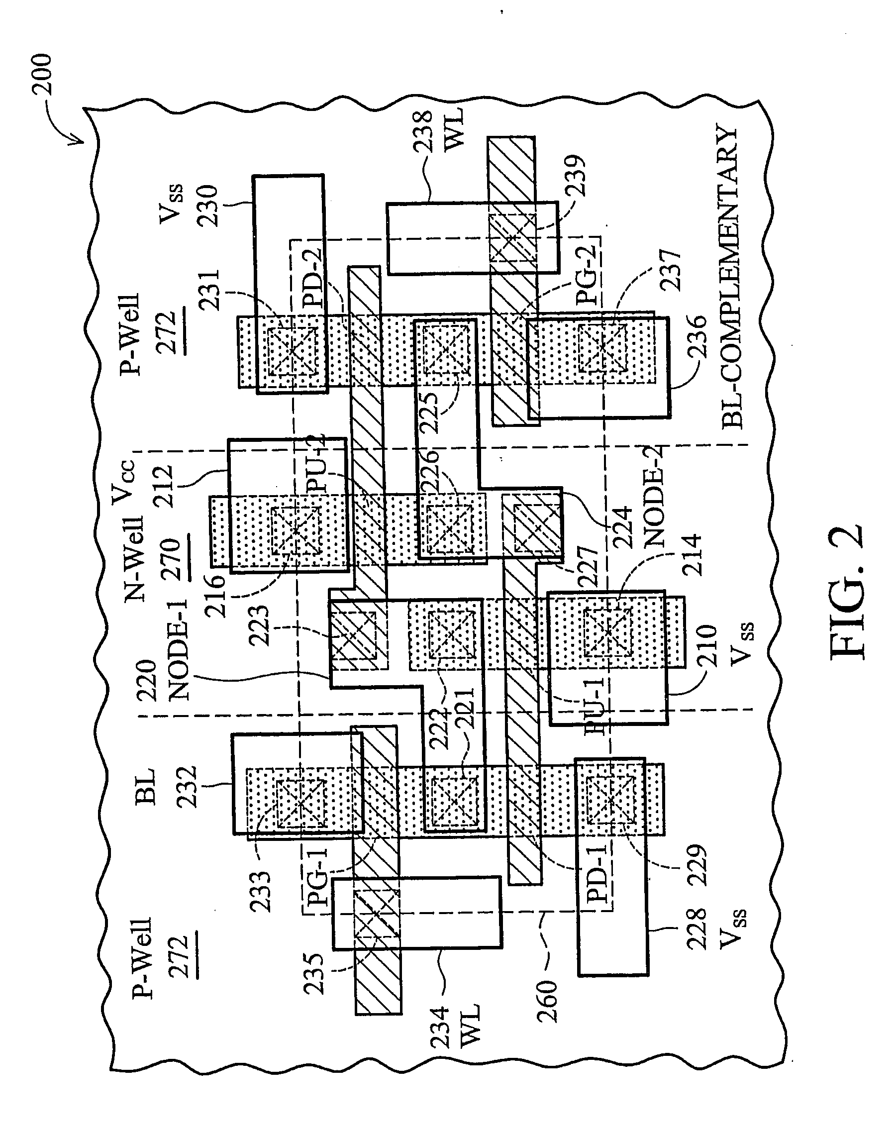
[0025] The making and using of the presently preferred embodiments are discussed in detail below. It should be appreciated, however, that the present invention provides many applicable inventive concepts that can be embodied in a wide variety of specific contexts. In particular, the method of the present invention is described in the context of a 6T-RAM. One of ordinary skill in the art, however, will appreciate that features of the present invention described herein may be used for forming other types of devices, such as an 8T-SRAM memory device, memory devices other than SRAMs, or semiconductor devices other than memory devices. Furthermore, embodiments of the present invention may be used as stand-alone memory devices, memory devices integrated with other integrated circuitry, or the like. Accordingly, the specific embodiments discussed herein are merely illustrative of specific ways to make and use the invention, and do not limit the scope of the invention.

[0026] Referring firs...


PUM


Abstract

A memory array with a row of strapping cells is provided. In accordance with embodiments of the present invention, strapping cells are positioned between two rows of a memory array. The strapping cells provide a P+strap between N+active areas of two memory cells in a column and provide an N+strap between P+active areas of two memory cells in a column of the memory array. The strapping cells provide an insulating structure between the two rows of the memory array and create a more uniform operation of the memory cells regardless of the positions of the memory cells within the memory array. In an embodiment, a dummy N-well may be formed along the outer edge of the memory array in a direction perpendicular to the row of strapping cells. Furthermore, transistors may be formed in the strapping cells to provide additional insulation between the strapped memory cells.

Description

TECHNICAL FIELD [0001] The present invention relates generally to semiconductor devices and, more particularly, to a memory cell layout for integrated circuits. BACKGROUND [0002] Generally, memory chips comprise an array of memory cells interconnected by bit lines and word lines. The word lines and bit lines are used to read and write binary values to each of the memory cells, wherein each memory cell represents a bit of information. Because each memory cell represents a bit of information and may be connected to other circuitry, it is desirable that the electrical and operational characteristics of all memory cells be consistent. [0003] The operational and electrical characteristics of memory cells, however, vary depending on where a memory cell is located within the layout of the memory array. For example, memory cells along the edge of the memory array may have different electrical and operational characteristics than memory cells located in the inner region of the memory array. ...

Claims


Application Information

Patent Timeline
IPC IPC(8): H01L29/76
CPCG11C11/412H01L27/1104H01L27/11Y10S257/903H10B10/00H10B10/12
Inventor LIAW, JHON-JHY
Owner TAIWAN SEMICON MFG CO LTD
Why Eureka
Try Eureka