Semiconductor packages, methods of forming semiconductor packages, and methods of cooling semiconductor dies

a technology of semiconductor dies and semiconductor components, applied in the direction of individual semiconductor device testing, semiconductor/solid-state device details, instruments, etc., can solve the problems of numerous difficulties encountered in attempting to adequately remove thermal energy from such integrated circuits, high heat generation during operation, and the use of conventional heat sinks made of black-coated metallic materials

Active Publication Date: 2007-09-06
MICRON TECH INC
View PDF17 Cites 53 Cited by
  • Summary
  • Abstract
  • Description
  • Claims
  • Application Information

AI Technical Summary

Problems solved by technology

High-performance integrated circuits (for example, microprocessors, network processors, and high-speed static random access memory (SRAM)) run at high clock speeds and have high standby currents, which can result in very high heat generation during operation.
Numerous difficulties are encountered in attempting to adequately remove thermal energy from such integrated circuits to avoid overheating of the circuits.
For i

Method used


Image

  • Semiconductor packages, methods of forming semiconductor packages, and methods of cooling semiconductor dies
  • Semiconductor packages, methods of forming semiconductor packages, and methods of cooling semiconductor dies
  • Semiconductor packages, methods of forming semiconductor packages, and methods of cooling semiconductor dies

Examples


Embodiment Construction

[0036] This disclosure of the invention is submitted in furtherance of the constitutional purposes of the U.S. Patent Laws “to promote the progress of science and useful arts” (Article 1, Section 8).

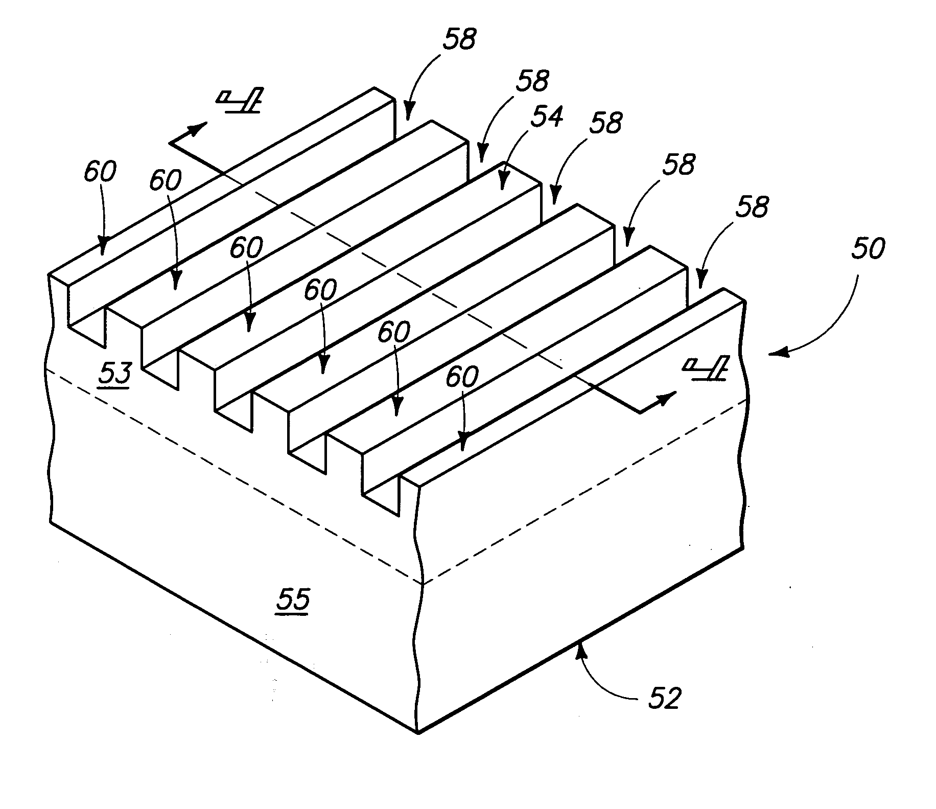
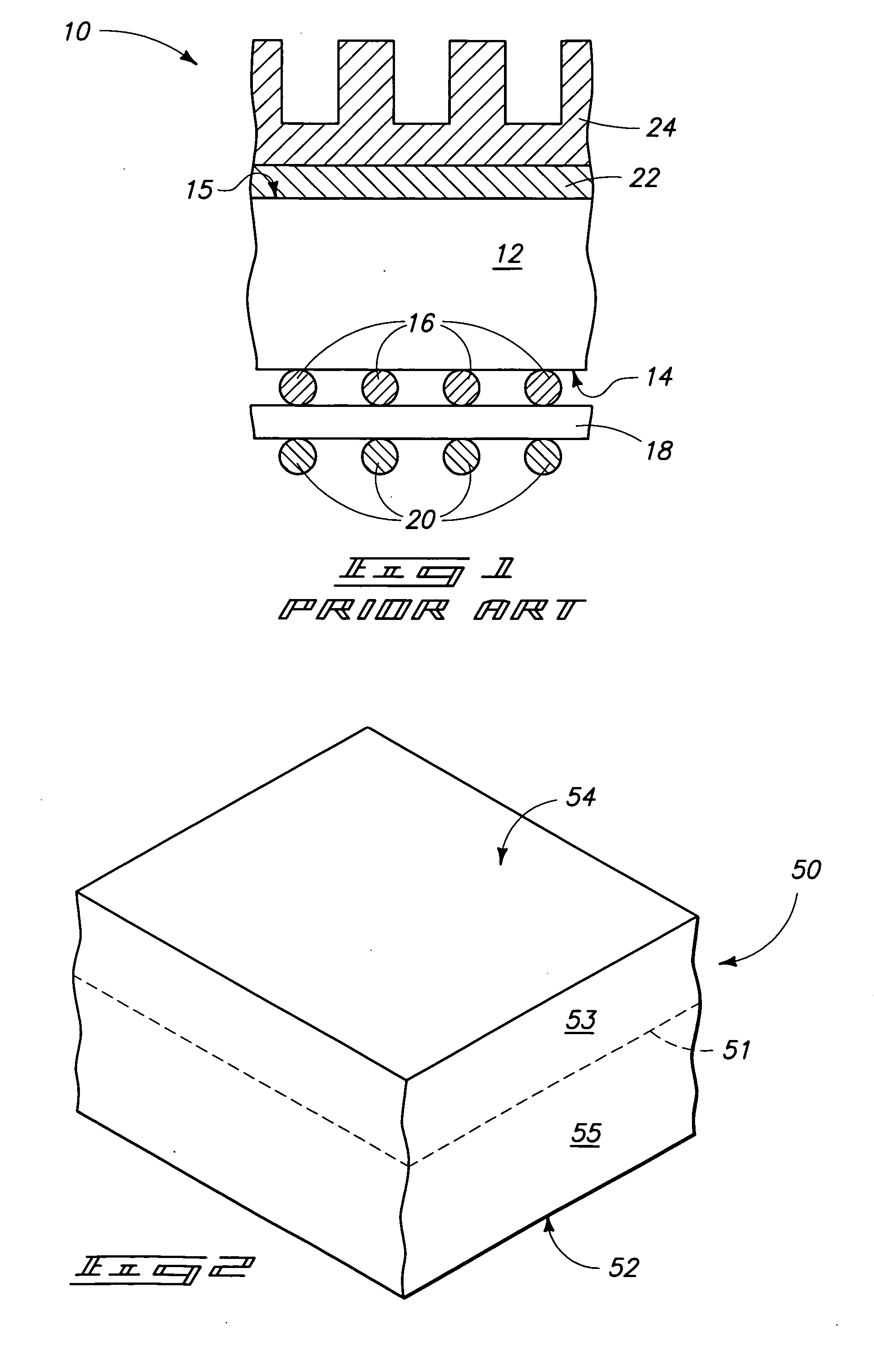
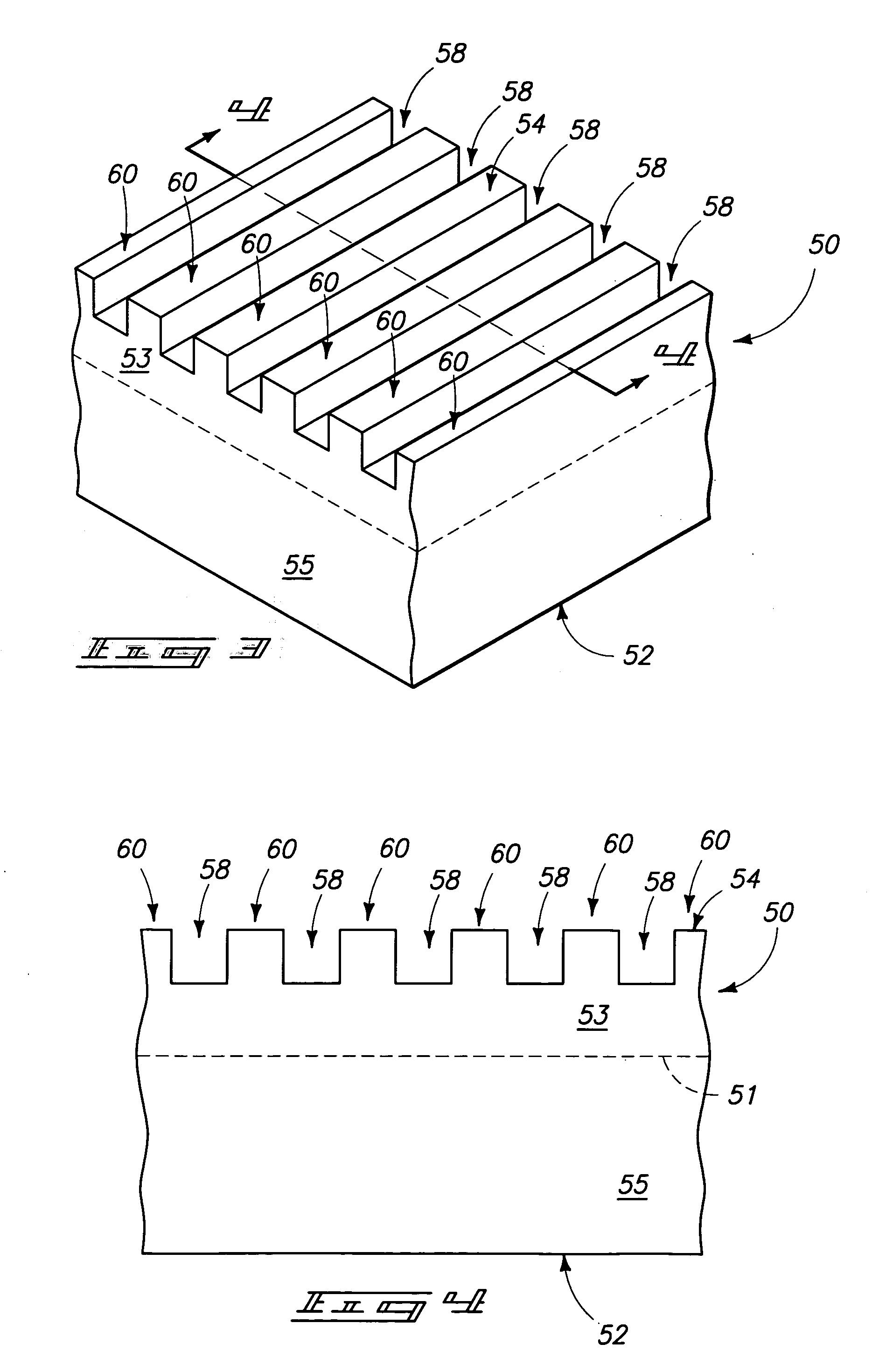
[0037] The invention includes semiconductor packages utilizing carbon nanotubes for thermal transfer, and includes methods for incorporating carbon nanotubes into semiconductor packages.

[0038] Carbon nanotubes can be insulating, semiconductive, or metallic in nature. The physical and electrical properties of carbon nanotubes can be influenced by the methodology utilized to grow the nanotubes. For instance, the bandstructure of carbon nanotubes can be dependent on the diameter of the tubes, the lattice structure within the tubes, the orientation of the tubes, and various other factors. However, it is generally recognized that carbon nanotubes having metal-like electrical properties can be relatively easily created. Specifically, it is recognized that large diameter nanotubes can have ne...


PUM


Abstract

The invention includes semiconductor packages having grooves within a semiconductor die backside; and includes semiconductor packages utilizing carbon nanostructures (such as, for example, carbon nanotubes) as thermally conductive interface materials. The invention also includes methods of cooling a semiconductor die in which coolant is forced through grooves in a backside of the die, and includes methods of making semiconductor packages.

Description

TECHNICAL FIELD [0001] The invention pertains to semiconductor packages, methods of forming semiconductor packages, and methods of cooling semiconductor dies. BACKGROUND OF THE INVENTION [0002] High-performance integrated circuits (for example, microprocessors, network processors, and high-speed static random access memory (SRAM)) run at high clock speeds and have high standby currents, which can result in very high heat generation during operation. Numerous difficulties are encountered in attempting to adequately remove thermal energy from such integrated circuits to avoid overheating of the circuits. [0003]FIG. 1 shows a prior art semiconductor package construction 10 illustrating conventional methodologies for cooling an integrated circuit. The construction includes an integrated circuit chip or die 12. Such die will comprise a semiconductor material substrate and various integrated circuit components associated with the substrate. The substrate can, for example, comprise, consis...

Claims


Application Information

Patent Timeline
IPC IPC(8): G01R31/26
CPCH01L23/367H01L23/3672H01L23/373Y10S977/742H01L2224/16H01L2224/73253H01L2924/10158H01L23/3733
Inventor MOULI, CHANDRASANDHU, GURTEJ S.
Owner MICRON TECH INC
Why Eureka
Try Eureka