Nonvolatile storage device and data writing method thereof
- Summary
- Abstract
- Description
- Claims
- Application Information
AI Technical Summary
Benefits of technology
Problems solved by technology
Method used
Image
Examples
first embodiment
[0088]A nonvolatile storage device according to the present embodiment holds, in an auxiliary memory, at least a single page worth of data on a sector unit which is inputted from an access device, and writes the data in a main memory on a page unit. In this manner, the number of writing times can be reduced. Thus, since creation of invalid pages can be reduced, the number of times of garbage collection can be reduced and the operation speed can be increased.
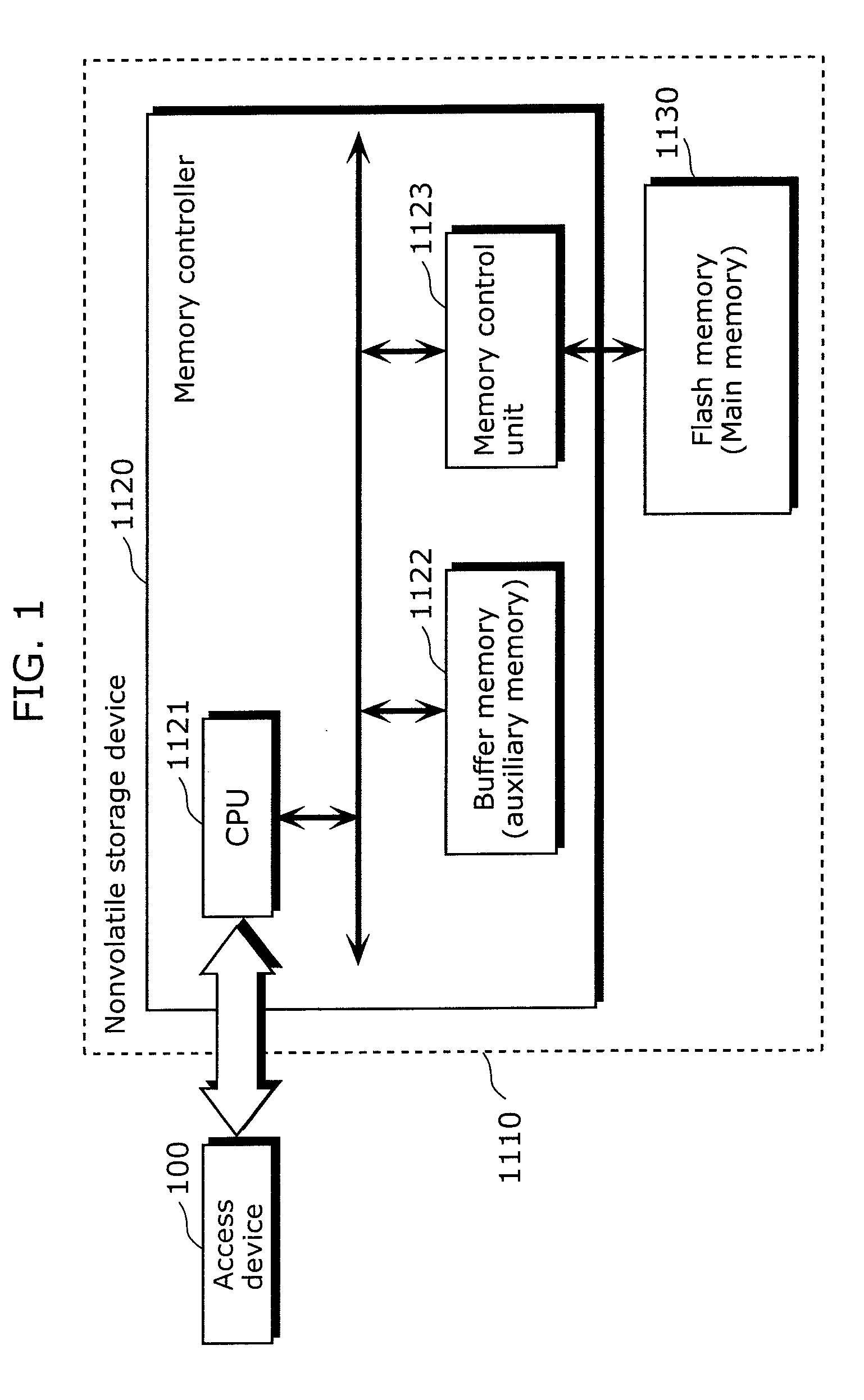
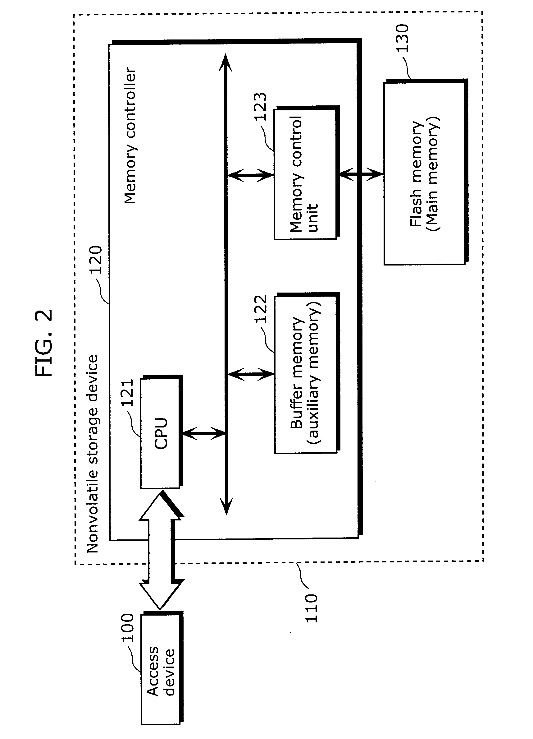
[0089]A configuration of the nonvolatile storage device according to the first embodiment of the present invention is described hereinafter.
[0090]FIG. 2 is a block diagram showing the configuration of a nonvolatile storage system according to the first embodiment of the present invention. The nonvolatile storage system shown in FIG. 2 includes a nonvolatile storage device 110 and an access device 100.
[0091]The access device 100 transmits a read or write command of user data on a sector unit (to be simply referred to as data herei...
second embodiment
[0127]In a nonvolatile storage device according to a second embodiment, when data including the identical logical address is held in the buffer memory 122, new data is overwritten in an area in which old data is held. In this manner, the capacity of the buffer memory 122 can be effectively utilized.
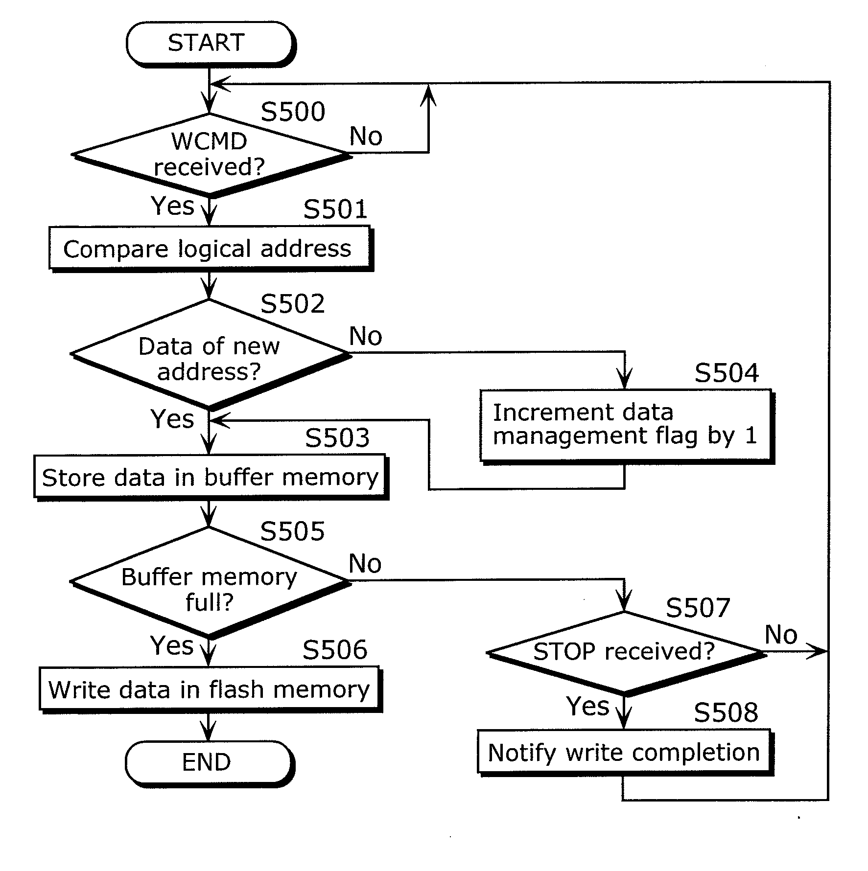
[0128]FIG. 10 is a flow chart of a write process of the nonvolatile storage device according to the second embodiment. Since the configuration of the nonvolatile storage device according to the second embodiment is the same as that in FIG. 2, a description thereof is omitted.
[0129]As shown in FIG. 10, a write process of the nonvolatile storage device according to the second embodiment is different from the write process in the first embodiment in that when data having the same logical sector address is present in the buffer memory 122 in Step S902 (No in S902), 1 sector worth of new data inputted from an access device 100 and a logical sector address of the data are overwritten in an area...
third embodiment
[0137]A nonvolatile storage device according to a third embodiment includes a notifying unit which notifies a CPU 121 that a buffer memory 122 is full. In this manner, the processes of the CPU 121 can be reduced.
[0138]FIG. 12 is a block diagram showing a configuration of a nonvolatile storage system according to the third embodiment. The reference numerals identical to that of FIG. 2 are used in FIG. 12, and the detailed description thereof is omitted.
[0139]The nonvolatile storage device 110 according to the third embodiment shown in FIG. 12 is different from that of the first embodiment shown in FIG. 2 in that a memory controller 120 includes a notifying unit 124. The notifying unit 124 is implemented by hardware, judges whether or not the buffer memory 122 is full, and notifies the CPU 121 of a result of the judgment. The CPU 121 controls the memory control unit 123 based on the result of the judgment notified by the notifying unit 124 and writes data held in the buffer memory 122...
PUM
 Abstract
Description
Claims
Application Information


