Fringe capacitor using bootstrapped non-metal layer

a non-metal layer, capacitor technology, applied in capacitors, semiconductor devices, semiconductor/solid-state device details, etc., can solve the problems of consuming a large area of the ic, and reducing the capacitance density of the fringe capacitor, etc., to achieve minimize or eliminate the parallel plate capacitor, maximize the fringe capacitor, and high density

Inactive Publication Date: 2007-09-20
MICROCHIP TECH INC
View PDF12 Cites 11 Cited by
  • Summary
  • Abstract
  • Description
  • Claims
  • Application Information

AI Technical Summary

Benefits of technology

[0009] In one set of embodiments, accurate high density capacitors may be constructed on an integrated circuit by using only fringe-capacitance developed between metal lines within a given metal layer and minimizing or completely eliminating parallel-plate-capacitance. In order to maximize fringe-capacitance, the metal lines comprising the top and bottom plates of the capacitor may be interdigitated with minimum spacing, and parallel-plate-capacitance may be minimized or eliminated by stacking top plate traces on top of each other and bottom plate traces on top of each other. Therefore, a top level layer in a multi-layer process may be used for routing, and all layers below the top level layer, including the bottom layer, may be configured as interdigitated structures to maximize capacitance density. In order to minimize capacitance developed between the top plate in the bottom metal layer and the substrate, a low-impedance conductive plate constructed in polysilicon layer may be inserted between the bottom metal layer and the substrate. In one embodiment, the polysilicon plate is bootstrapped to the top plate to drive the polysilicon-to-substrate capacitance and minimize or eliminate any charge transfer from the top plate to the polysilicon plate. Bootstrapping the polysilicon plate to the top plate may also minimize and / or eliminate the bottom-plate-to-substrate capacitance, and all metal layers that are not used for routing may be used in constructing the capacitor(s).

Problems solved by technology

Such structures, however, oftentimes consume a large area of the IC.
In contrast, the capacitance between the various metal layers may not be as effectively controlled, since the thickness of the field-oxide region in the corresponding metal-‘field-oxide’-metal structure can generally vary from lot to lot and across a die / wafer.
A minimal ‘top-plate’-to-substrate capacitance is preferable because such a capacitance can be a source of errors in switched capacitor circuits.
This, however, reduces the capacitance density of the fringe-capacitance, since the bottom metal layer cannot be used when forming the desired fringe-capacitance.

Method used


Image

  • Fringe capacitor using bootstrapped non-metal layer
  • Fringe capacitor using bootstrapped non-metal layer
  • Fringe capacitor using bootstrapped non-metal layer

Examples


Embodiment Construction

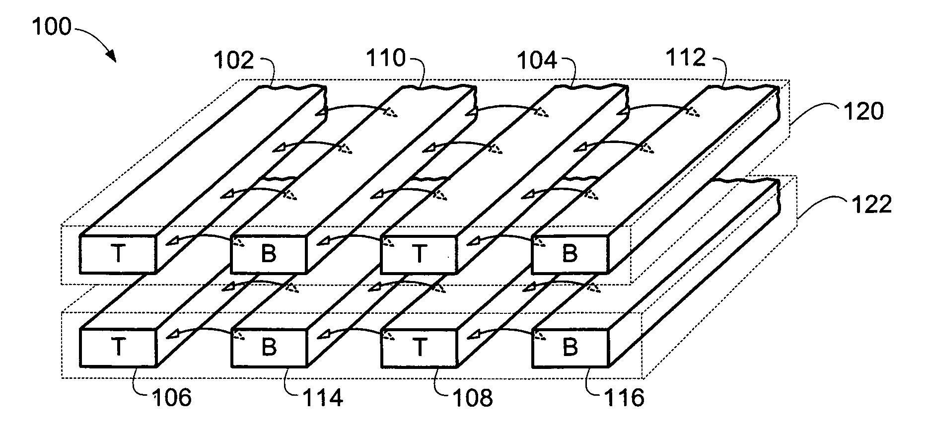
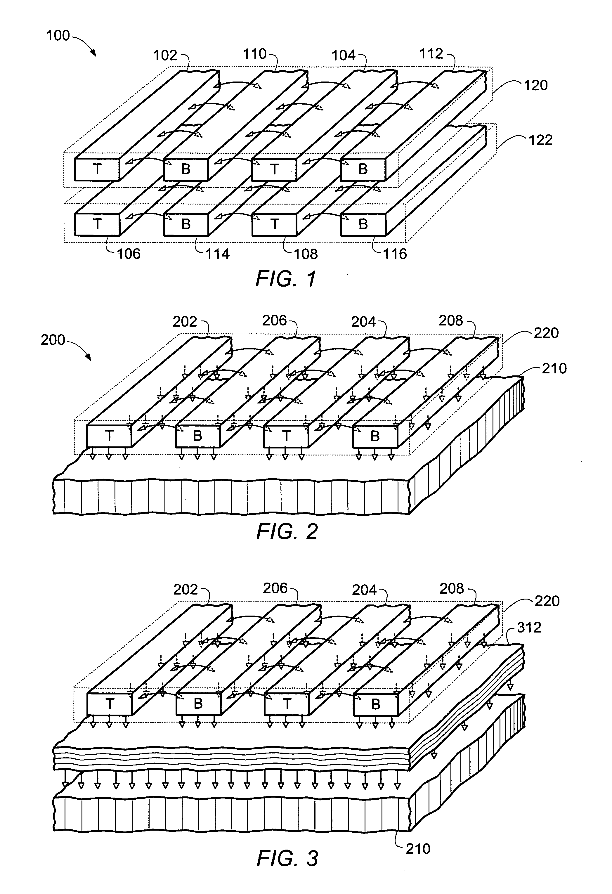
[0020] When using only fringe-capacitance between metal lines within a given metal layer in constructing metal-to-metal capacitors on an integrated circuit (IC), the ability for matching of unit capacitors may be superior to the matching of unit capacitors whose configuration also includes parallel-plate-capacitance. Likewise, higher capacitive densities may be achieved with capacitors configured using solely fringe-capacitance than with capacitors that also comprise parallel-plate structures. In order to maximize fringe-capacitance, the metal lines or strips used for top and bottom plates of the capacitor may be interdigitated with minimum spacing. Furthermore, by stacking top plate traces on top of each other and bottom plate traces on top of each other, the parallel—or layer to layer—capacitance may be minimized. Thus, a top level layer in a multi-layer process may be used for routing, and all layers below the top level layer, including the bottom layer, may be configured as inte...


PUM


Abstract

Capacitors configured in a switched-capacitor circuit on a semiconductor device may comprise very accurately matched, high capacitance density metal-to-metal capacitors, using top-plate-to-bottom-plate fringe-capacitance for obtaining the desired capacitance values. A polysilicon plate may be inserted below the bottom metal layer as a shield, and bootstrapped to the top plate of each capacitor in order to minimize and/or eliminate the parasitic top-plate-to-substrate capacitance. This may free up the bottom metal layer to be used in forming additional fringe-capacitance, thereby increasing capacitance density. By forming each capacitance solely based on fringe-capacitance from the top plate to the bottom plate, no parallel-plate-capacitance is used, which may reduce capacitor mismatch. Parasitic bottom plate capacitance to the substrate may also be eliminated, with only a small capacitance to the bootstrapped polysilicon plate remaining. The capacitors may be bootstrapped by coupling the top plate of each capacitor to a respective one of the differential inputs of an amplifier comprised in the switched-capacitor circuit.

Description

BACKGROUND OF THE INVENTION [0001] 1. Field of the Invention [0002] This invention relates generally to the field of semiconductor circuit design, and more particularly to the design of a capacitor structure on a semiconductor substrate. [0003] 2. Description of the Related Art [0004] Many integrated circuits (ICs), including mixed-signal circuits that include both digital and analog components, oftentimes require high-performance capacitors configured on the chip. Currently, a wide variety of applications for example dynamic random access memories, phase-locked loops, voltage controlled oscillators, operational amplifiers, and switched capacitor circuits—feature capacitors formed on integrated circuits. Generally, these on-chip capacitors can also be used to decouple digital and analog integrated circuits from potential noise that may be generated by the rest of the system. In many of the present systems, on-chip capacitors are designed as metal-to-metal capacitors due to the advan...

Claims


Application Information

Patent Timeline
Patent Type & Authority Applications(United States)
IPC IPC(8): H01L29/94
CPCH01L23/5223H01L28/87H01L2924/3011H01L2924/0002H01L2924/00
Inventor MCLEOD, SCOTT C.
Owner MICROCHIP TECH INC
Why Eureka
Try Eureka