
Memory system and method of controlling the memory system

Inactive Publication Date: 2007-09-20
KK TOSHIBA
View PDF6 Cites 6 Cited by
  • Summary
  • Abstract
  • Description
  • Claims
  • Application Information

AI Technical Summary

Problems solved by technology

Many copy operation for data items not to be written will greatly increase the overhead in the data-rewriting process.
As mentioned above, the access speed changes in accordance with the address that is accessed, resulting in possible fluctuation of the process time of the memory in response to an access.
As a result, the performance of the memory card deteriorates depending on the address that the host apparatus accesses.

Method used


Image

  • Memory system and method of controlling the memory system
  • Memory system and method of controlling the memory system
  • Memory system and method of controlling the memory system

Examples


first embodiment

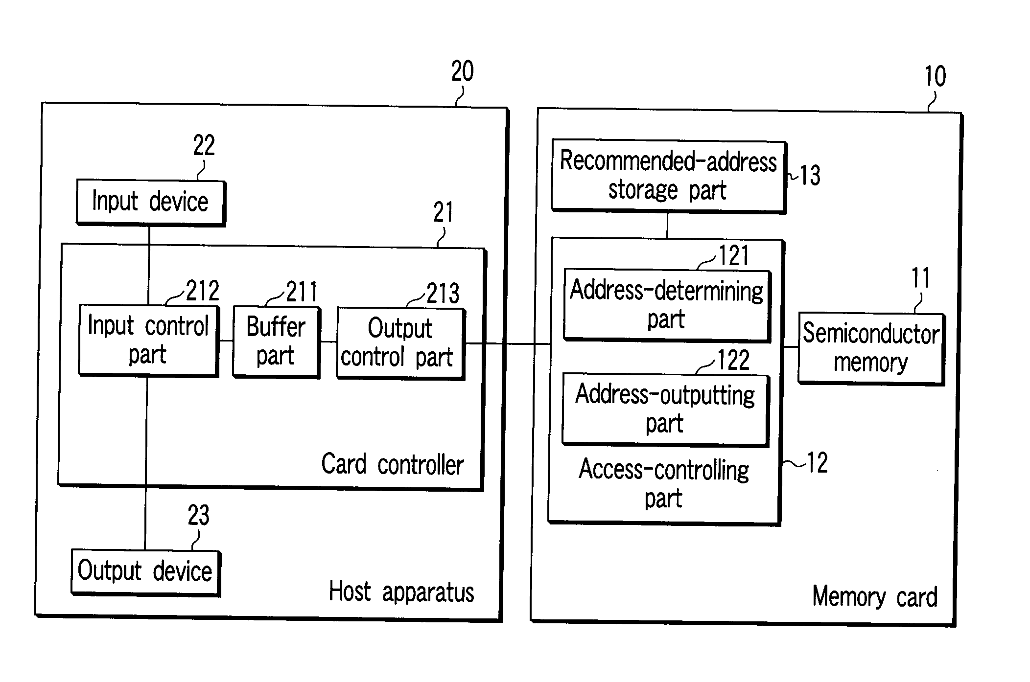
[0026] As shown in FIG. 1, the memory card according to the first embodiment of this invention is a memory card 10 that can transmit data to and receive from a host apparatus 20. The memory card 10 comprises a semiconductor memory 11 and an access control part 12. The semiconductor memory 11 can be accessed from the host apparatus 20. The access control part 12 determines a recommended address to be accessed, from the operation information about the memory card 10. The recommended address thus determined is output to the host apparatus 20. Data to which the recommended address is allocated is read from, or written into, the semiconductor memory 11. Data to which the recommended address is allocated can be written faster than data with any other addresses at the time certain data writing is completed. The “operation information” represents a factor that influences the process time in response to an access to the semiconductor memory 11, such as the data-storage state or the functions...

second embodiment

[0063] As FIG. 12 shows, a memory card 100 according to the second embodiment of the present invention comprises a semiconductor memory 110 and a memory controller 120. The memory card 100 can be coupled to a host apparatus 20. The host apparatus 20, which is shown in FIG. 12, is identical in configuration to the host apparatus 20 shown in FIG. 1.

[0064] Like the semiconductor memory 11 according to the first embodiment, the semiconductor memory 110 has its access speed changed in accordance with the address that has been accessed. The semiconductor memory 110 comprises a memory core 111, an access-controlling circuit 112, and a recommended-address storing circuit 113. The memory core 111 is constituted by, for example, districts D1 to D3 as shown in FIG. 9 or FIGS. 10A to 10D. The access-controlling circuit 112 selects recommended addresses in accordance with the operation information about the memory core 111. The access-controlling circuit 112 comprises an address-selecting circu...


PUM


Abstract

A memory system for transmitting data to and receiving data from a host apparatus includes a semiconductor memory and an access-controlling part. The semiconductor memory has storage areas identified by physical addresses, stores data in each of the storage areas, performs data write in accordance with a request made by the host apparatus. The access-controlling part selects a recommended address, which is recommended to be used in a next data write, on the basis of operation information about a factor that influences time consumed for data write in the semiconductor memory, and outputs the recommended address to the host apparatus.

Description

CROSS-REFERENCE TO RELATED APPLICATIONS [0001] This application is based upon and claims the benefit of priority from prior Japanese Patent Application No. 2006-072956, filed Mar. 16, 2006, the entire contents of which are incorporated herein by reference. BACKGROUND OF THE INVENTION [0002] 1. Field of the Invention [0003] The present invention relates to a memory system that transmits data to and receives data from a host apparatus and a method of controlling the memory system. [0004] 2. Description of the Related Art [0005] A semiconductor memory such as a NAND-type flash memory, from and into which some data items of a predetermined size can be read and written, may be incorporated in a memory card that is to be connected to a host apparatus (See, for example, Jpn. Pat. Appln. KOKAI Publication No. 7-122088.). In such a semiconductor memory, the process time in response to an access may vary in accordance with the address of the memory to which the host apparatus accesses. The “p...

Claims


Application Information

Patent Timeline
IPC IPC(8): G06F13/00
CPCG11C16/12G11C16/08
Inventor OSHIMA, TAKASHI
Owner KK TOSHIBA
Features
  • Generate Ideas
  • Intellectual Property
  • Life Sciences
  • Materials
  • Tech Scout
  • Unparalleled Data Quality
  • Higher Quality Content
  • 60% Fewer Hallucinations
Learn More