
Semiconductor device provided with function for screening test regarding operating speed

Inactive Publication Date: 2007-09-20
FUJITSU SEMICON LTD
View PDF10 Cites 4 Cited by
  • Summary
  • Abstract
  • Description
  • Claims
  • Application Information

AI Technical Summary

Benefits of technology

[0016] According to at least one embodiment of the present invention, the margin detecting circuit is provided for the first flip-flop in the semiconductor device, so that the margin detecting circuit displaces the timing of one of a data signal and a synchronizing clock signal, and causes the second flip-flop to load the data signal in response to the synchronizing clock signal whose relative timing is displaced, followed by checking whether data loading is properly performed. With this provision, a check can be made as to whether a sufficient margin exists for the first flip-flop in the semiconductor device. The operating frequency is increased in a stepwise manner while monitoring whether a sufficient margin exists. The operating frequency observed at the time it is determined that there is no sufficient margin serves as an indication of the operating frequency at which the semiconductor device can properly operate at maximum speed. This provision makes it possible to perform a highly-accurate screening test regarding operating speed with a small amount of time and labor.

Problems solved by technology

Because of such labor, a substantial amount of time and costs is required to perform a screening test regarding operating speed with high precision.

Method used


Image

  • Semiconductor device provided with function for screening test regarding operating speed
  • Semiconductor device provided with function for screening test regarding operating speed
  • Semiconductor device provided with function for screening test regarding operating speed

Examples


Embodiment Construction

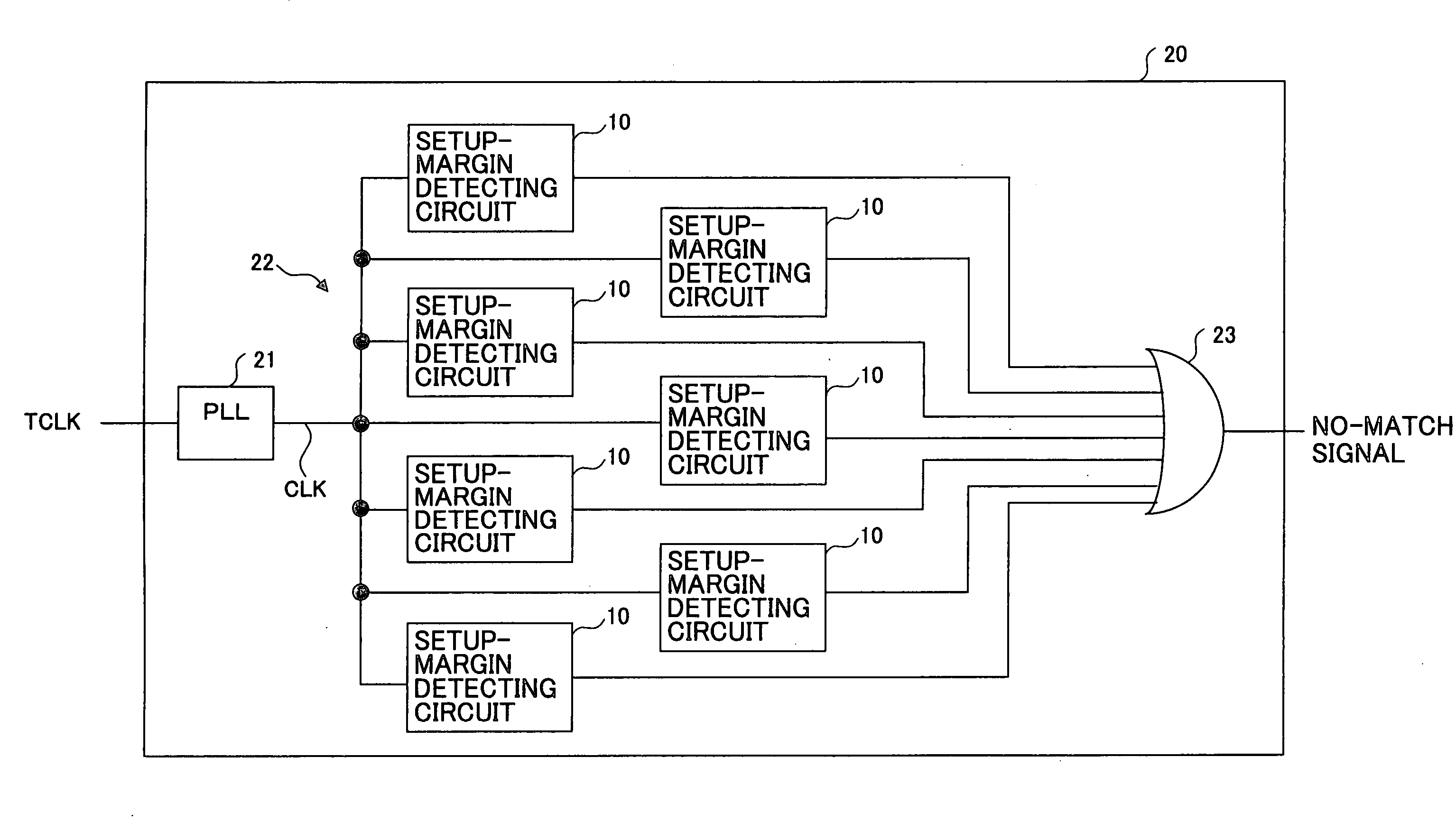
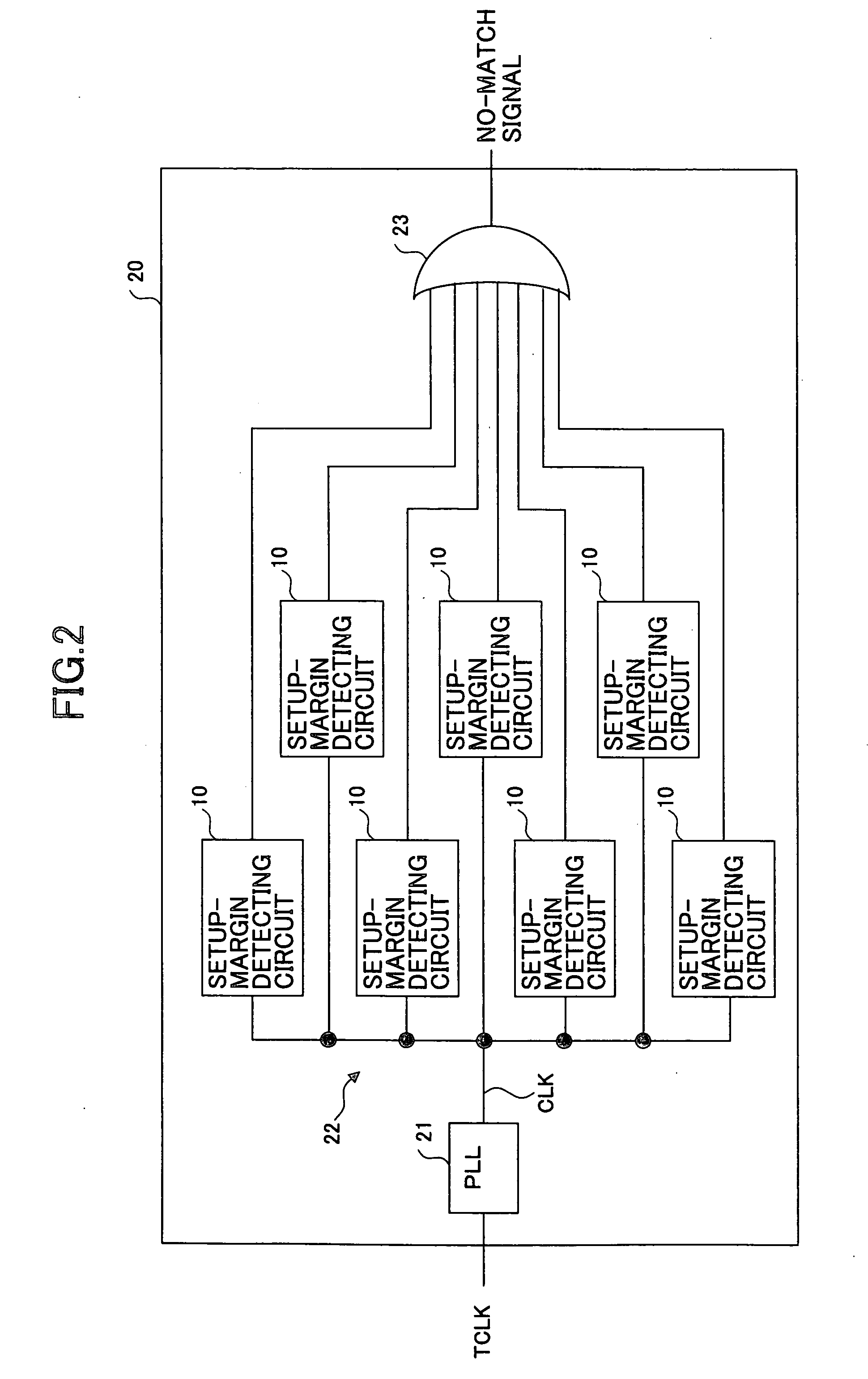
[0022] In the following, embodiments of the present invention will be described with reference to the accompanying drawings.

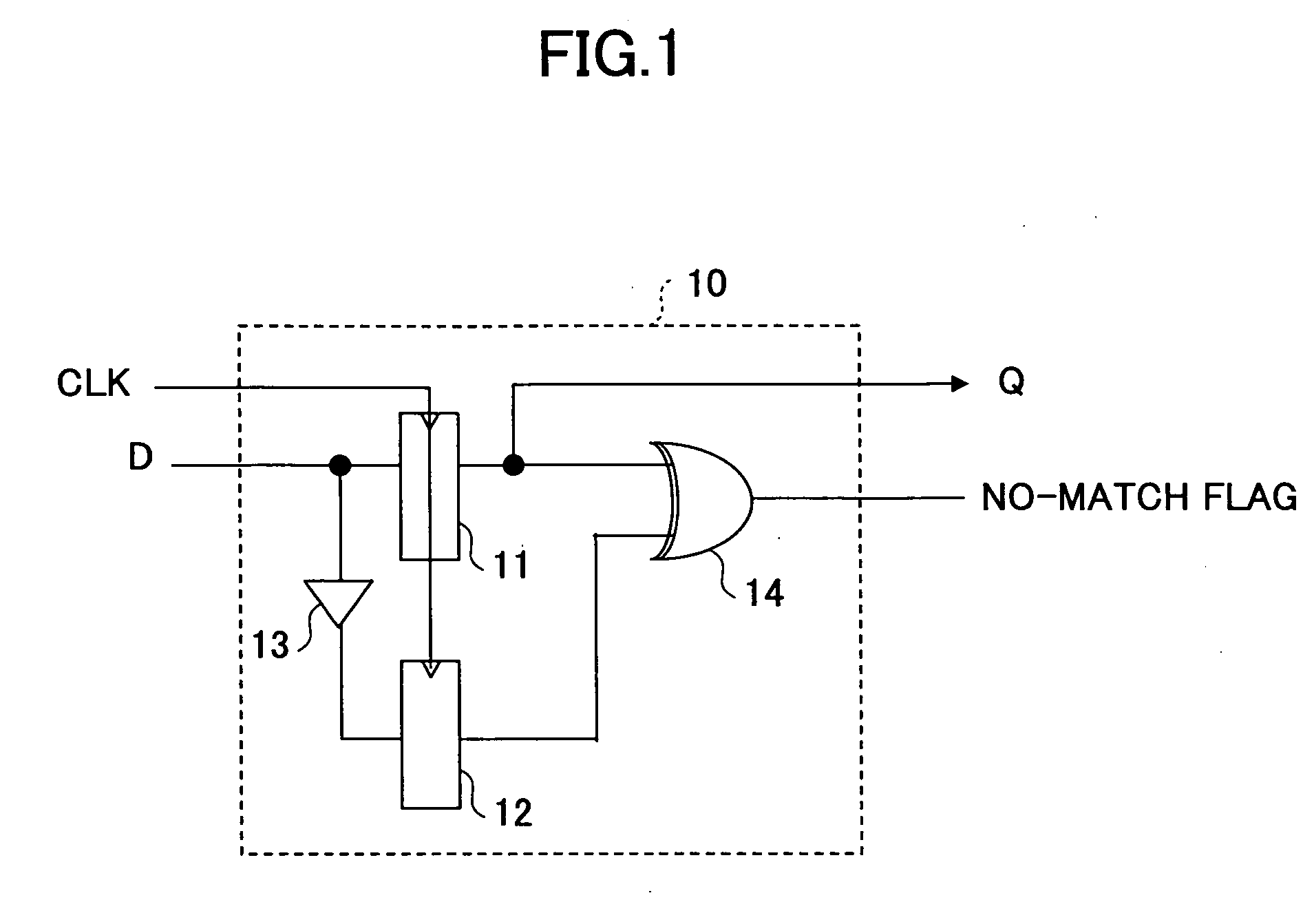
[0023] The present invention provides a margin detecting circuit, which will later be described, to all or some of flip-flops provided in the semiconductor device. When the margin detecting circuits are to be provided to only some of the flip-flops in the semiconductor device, these flip-flops may be those situated along critical paths on which the conditions for proper operation are tight with respect to timing. Namely, if there are 10,000 paths including flip-flops, for example, a predetermined number of paths on which timing is believed to be most tight among the 10,000 paths may be selected, and the margin detecting circuits may be attached to those selected paths.

[0024] A single margin detecting circuit is provided in one-to-one correspondence to each flip-flop (hereinafter referred to as a first flip-flop), and includes a flip-flop (hereinafter referred...


PUM


Abstract

A semiconductor device includes one or more margin detecting circuits, each of which includes a first flip-flop having a first clock signal input node coupled to a clock supply node and a first data input node coupled to a data supply node, a second flip-flop having a second clock signal input node coupled to the clock supply node and a second data input node coupled to the data supply node, a delay element situated between the clock supply node and the second clock input node or between the data supply node and the second data input node, and a check circuit configured to check whether data stored in the first flip-flop matches data stored in the second flip-flop.

Description

CROSS-REFERENCE TO RELATED APPLICATIONS [0001] The present application is based upon and claims the benefit of priority from the prior Japanese Patent Application No. 2006-075004 filed on Mar. 17, 2006, with the Japanese Patent Office, the entire contents of which are incorporated herein by reference. BACKGROUND OF THE INVENTION [0002] 1. Field of the Invention [0003] The present invention generally relates to semiconductor devices and tests for semiconductor devices, and particularly relates to a semiconductor device equipped with a test function and a test method using such a semiconductor device. [0004] 2. Description of the Related Art [0005] Semiconductor devices such as RAM (Random Access Memory), CPU (Central Processing Unit), and FPGA (Field Programmable Gate Array) are subjected to a screening test regarding operation speed prior to shipment from the factory. In such a screening test regarding operation speed, an LSI tester is used to monitor the output data while changing ...

Claims


Application Information

Patent Timeline
IPC IPC(8): G01R31/28
CPCG01R31/30G11C29/50G01R31/31725G01R31/31718
Inventor OGAWA, TOSHIO
Owner FUJITSU SEMICON LTD
Features
  • Generate Ideas
  • Intellectual Property
  • Life Sciences
  • Materials
  • Tech Scout
  • Unparalleled Data Quality
  • Higher Quality Content
  • 60% Fewer Hallucinations
Learn More