Micro-element package module and manufacturing method thereof

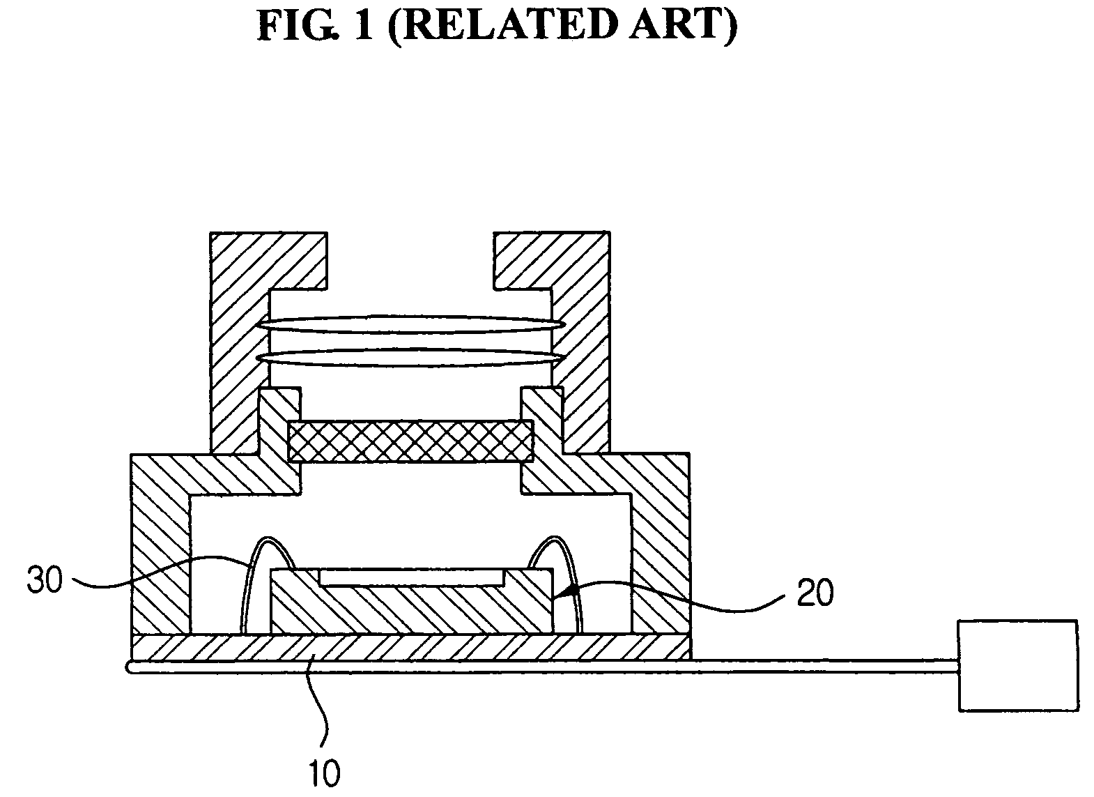
a technology of micro-elements and packaging modules, which is applied in the direction of electrical equipment, semiconductor devices, radio frequency controlled devices, etc., can solve the problems of affecting the quality of micro-elements, the method may not be applicable to thin-walled devices, and the manufacturing cost may increase, so as to reduce the size of the package module and reduce the bonding area

Inactive Publication Date: 2007-10-04
SAMSUNG ELECTRONICS CO LTD
View PDF6 Cites 20 Cited by
  • Summary
  • Abstract
  • Description
  • Claims
  • Application Information

AI Technical Summary

Benefits of technology

[0012]The present invention provides a micro-element package module which can reduce a size of a package module by reducing a bonding area, and also can form a thin module using a wafer-level-package (WLP) process, and a method of manufacturing the micro-element package module.

Problems solved by technology

Also, the method may not be applicable to a device which is manufactured thin and in a small size.
Accordingly, productivity may be deteriorated and manufacturing costs may be increased.
Also, in the case of the image sensor module constructed as above, a yield may be deteriorated due to contamination by particles during a manufacturing process.

Method used


Image

  • Micro-element package module and manufacturing method thereof
  • Micro-element package module and manufacturing method thereof
  • Micro-element package module and manufacturing method thereof

Examples


Embodiment Construction

[0032]Reference will now be made in detail to exemplary embodiments of the present invention, examples of which are illustrated in the accompanying drawings, wherein like reference numerals refer to the like elements throughout. The exemplary embodiments are described below in order to explain the present invention by referring to the figures.

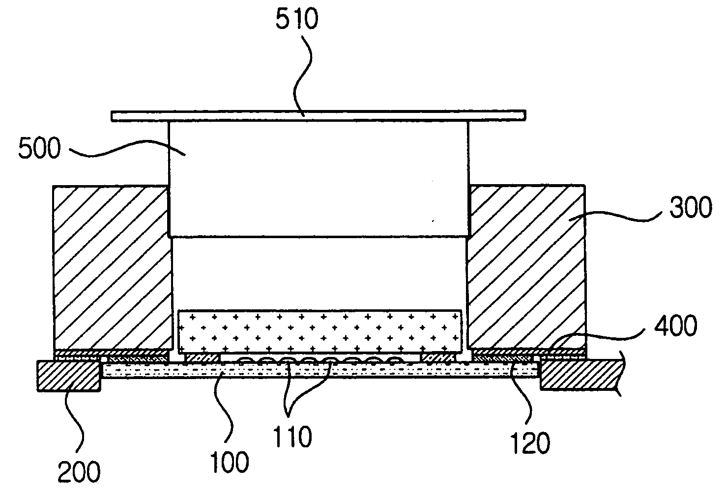
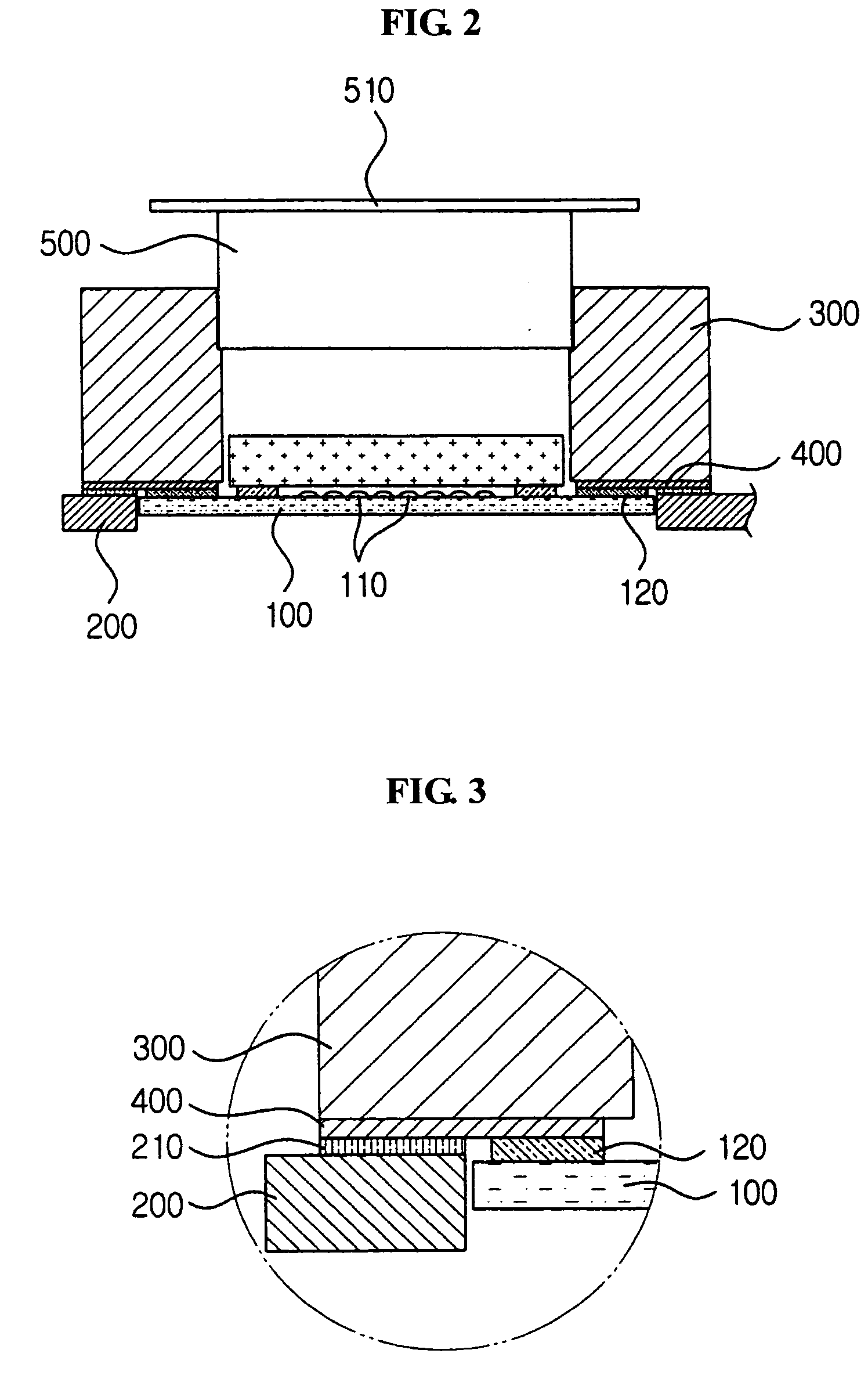
[0033]FIG. 2 is a cross-sectional view illustrating a structure of a micro-element package module according to an exemplary embodiment of the present invention, FIG. 3 is a partially enlarged view of a connecting portion of elements shown in FIG. 2, and FIG. 4 is a top view illustrating a structure of a micro-element package module according to an exemplary embodiment of the present invention.

[0034]As shown in FIGS. 2 through 4, the micro-element package module according to the exemplary embodiment of the present invention includes: an element substrate 100 having a micro-element 110 on a top surface of the element substrate 100; a circuit subs...


PUM


Abstract

A micro-element package module which can reduce manufacturing costs and can be advantageous for mass production due to simplifying its structure and manufacturing process, and also can facilitate miniaturization and promote thinness, and a method of manufacturing the micro-element package module. The micro-element package module includes: an element substrate having a micro-element on a top surface of the element substrate; a circuit substrate that is provided around the element substrate; and an element housing that is provided above the element substrate and the circuit substrate, and includes a connecting section for electrically connecting the micro-element and the circuit substrate.

Description

CROSS-REFERENCE TO RELATED APPLICATION[0001]This application claims priority from Korean Patent Application No. 10-2006-0030274, filed on Apr. 3, 2006, in the Korean Intellectual Property Office, the disclosure of which is incorporated herein by reference.BACKGROUND OF THE INVENTION[0002]1. Field of the Invention[0003]Apparatuses and methods consistent with the present invention relates to a micro-element package and a method of manufacturing the micro-element package, and more particularly, to a micro-element package module which can reduce manufacturing costs, can be advantageous for mass production due to simplifying its structure and manufacturing process, and also can facilitate miniaturization and promote thinness, and a method of manufacturing the micro-element package.[0004]2. Description of Related Art[0005]An image sensor is a device which changes light into an electrical signal and utilized in various fields of our daily lives.[0006]The image sensor includes a light recei...

Claims


Application Information

Patent Timeline
Patent Type & Authority Applications(United States)
IPC IPC(8): H01L33/00
CPCH01L27/14618H01L27/14685H01L27/14625H01L2224/48091H01L2224/48227H01L2924/00014H01L27/146
Inventor CHOI, MIN SEOGLEE, SEUNG WANKIM, WOON BAEJUNG, KYU DONG
Owner SAMSUNG ELECTRONICS CO LTD
Why Eureka
Try Eureka