
Electro-optical device, method for driving electro-optical device, and electronic apparatus

a technology of electrooptical devices and optical devices, applied in the direction of instruments, static indicating devices, etc., can solve problems such as complicated signal processing, and achieve the effects of high quality display, high contrast, and high display quality

Inactive Publication Date: 2007-10-04
SEIKO EPSON CORP
View PDF15 Cites 18 Cited by
  • Summary
  • Abstract
  • Description
  • Claims
  • Application Information

AI Technical Summary

Benefits of technology

[0008]An advantage of the present invention is to provide an electro-optical device that is capable of controlling luminance in accordance with a ratio of a light-emission area to an entire display without changing a voltage applied, and can achieve a high quality display by preventing flickering occurrence, and a method for driving the electro-optical device, and an electronic apparatus having the electro-optical device.
[0009]An electro-optical device according to a first aspect of the invention includes a plurality of pixels, a plurality of write scan lines including a predetermined number of the plurality of pixels as a unit, and a drive device driving the plurality of write scan lines non-sequentially and adjusting a light-emission period of the plurality of pixels in accordance with a luminance ratio of an image.
[0010]According to the first aspect of the invention, the light-emission period of the plurality of pixels is adjusted in accordance with the luminance ratio of the image to be displayed (a ratio of a light-emission area to an entire display). Therefore, it is possible to make the light-emission period long when the luminance ratio is small and make the light-emission period short when the luminance ratio is large, for example. As a result, luminance can be controlled in accordance with the luminance ratio of the image to be displayed without changing an applied voltage, thereby providing highly contrasted images as a CRT does. Further, according to the first aspect of the invention, the plurality of write scan lines including the predetermined number of the plurality of pixels as a unit are driven non-sequentially so as to disperse the pixels that are emitting light in an area having the pixels (viewing area). Therefore, even if the light-emission period of the pixels is adjusted to control luminance in accordance with the luminance ratio of the image to be displayed, occurrence of flickering is prevented, thereby providing a high quality display.
[0011]Here, the luminance ratio of the image to be displayed mentioned above refers to a ratio of an integrated luminance when all pixels in the viewing area of the electro-optical device produce luminescence at a maximum to an integrated luminance when only some pixels required to display in accordance with the image produce luminescence. Assuming that Lmax represents maximum luminance of an individual pixel and Lk (k is the number of pixels that are required to produce luminescence in accordance with an image) represents luminance of the individual pixel when only required pixels produce luminescence, the luminance ratio Lr of the image satisfies the formula below:Lr=ΣLk / ΣLmax and the ratio Lr falls within the range of 0 to 1 inclusive.
[0012]Further, driving the plurality of write scan lines non-sequentially refers to a drive other than sequential drives in a sequential order. Specifically, for example, a drive of interlacing a plurality of write scan lines spatially, a drive of interlacing a plurality of write scan lines in terms of time, and a drive of interlacing a plurality of write scan lines spatially and in terms of time are cited.
[0013]Further, an electro-optical device according to a second aspect of the invention includes a plurality of pixels and a drive device adjusting a light-emission period of the plurality of pixels in accordance with a luminance ratio of an image.

Problems solved by technology

The method of related art therefore makes signal processing complicated.

Method used


Image

  • Electro-optical device, method for driving electro-optical device, and electronic apparatus
  • Electro-optical device, method for driving electro-optical device, and electronic apparatus
  • Electro-optical device, method for driving electro-optical device, and electronic apparatus

Examples


first embodiment

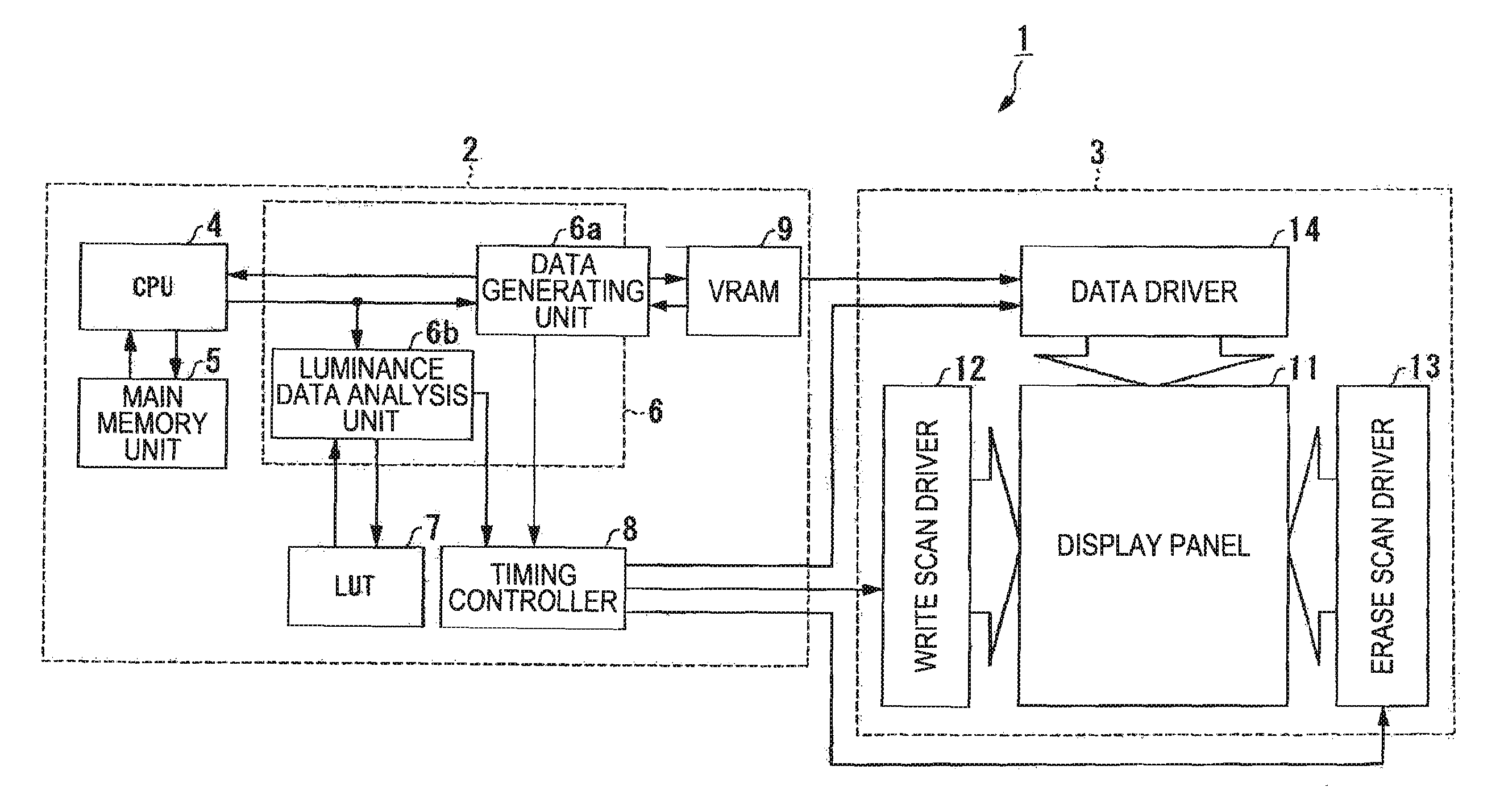
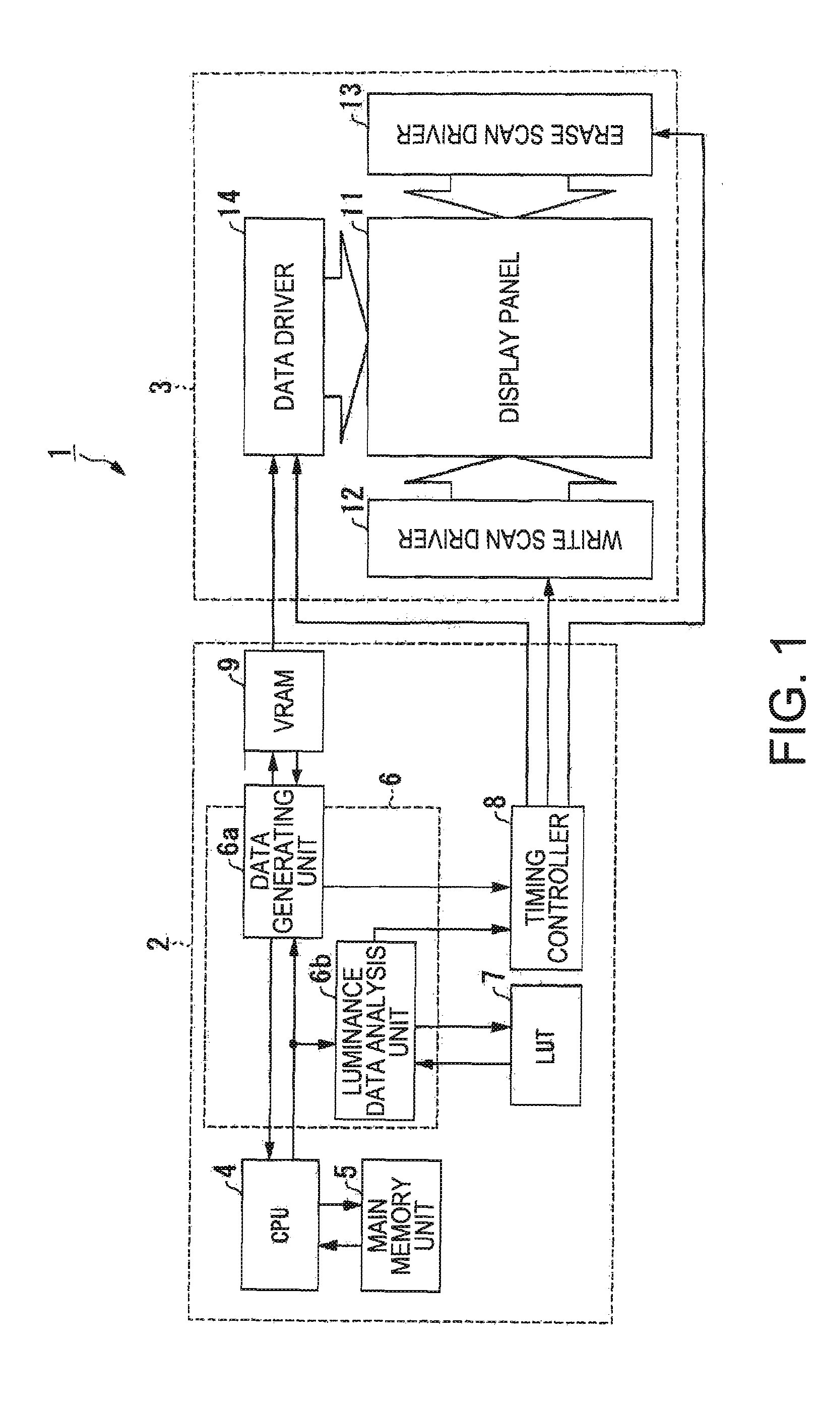
[0072]FIG. 1 is a block diagram illustrating an electrical structure of an electro-optical device according to a first embodiment of the invention. As the electro-optical device, an organic EL device is exemplified to describe below. Referring to FIG. 1, an organic EL device 1 as the electro-optical device includes a peripheral drive device 2 and a display panel unit 3. The peripheral drive device 2 includes a central processing unit (CPU) 4, a main memory unit 5, a graphics controller 6, a lookup table (LUT) 7, a timing controller 8 and a video RAM (VRAM) 9. The CPU 4 may be replaced with a microprocessor unit (MPU). The display panel unit 3 includes a display panel 1, a write scan driver 12, an erase scan driver 13, and a data driver 14.

[0073]The CPU included in the peripheral drive device 2 reads image data stored in the main memory unit 5, carries out various types of processing, such as expansion, with the main memory unit 5, and outputs processed data to the graphics controlle...

second embodiment

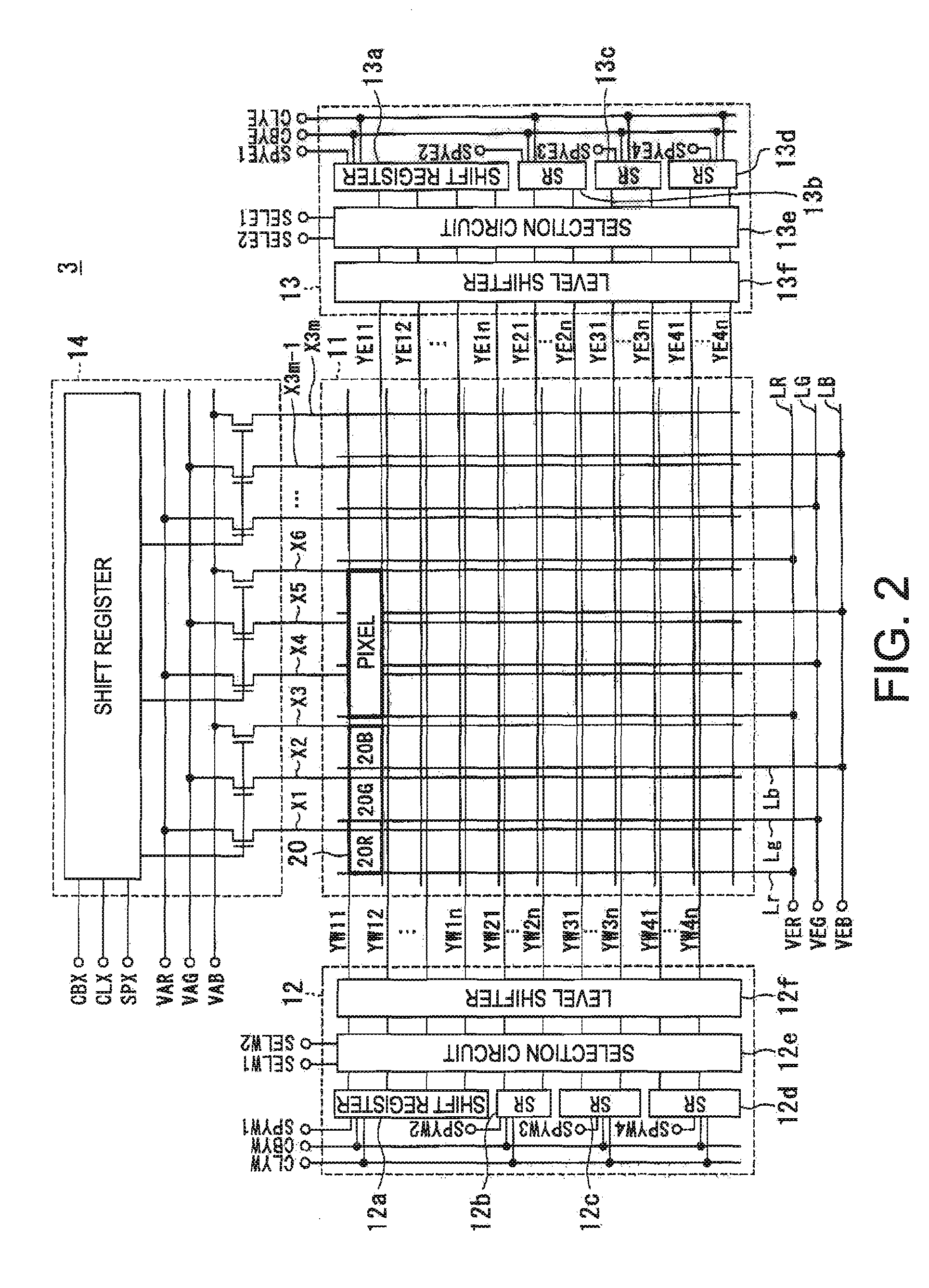
[0148]Next, an electro-optical device according to a second embodiment of the invention will be described. In this embodiment, an organic EL device is exemplified as the electro-optical device to describe. The electro-optical device according to the embodiment has almost the same structure as a whole as the electro-optical device of the first embodiment shown in FIG. 1. However, in the electro-optical device according to this embodiment, internal structures of which corresponding to the write scan driver 12 and the erase scan driver 13, and a signal output to which corresponding to the write scan driver 12 and the erase scan driver 13 from the timing controller 8 are different from those in the first embodiment. As for a description below, structural elements common to those of the electro-optical device 1 of the first embodiment are given the same numerals, and differences from the first embodiment will be explained.

[0149][Display Panel Unit 3]

[0150]FIG. 12 is a block diagram illus...

third embodiment

[0179]FIGS. 14A through 14C are diagrams for explaining a method for driving an electro-optical device according to a third embodiment of the invention. In these diagrams, the horizontal direction indicates a lapse of time and the vertical direction indicates the scan direction of the scan lines as those in FIGS. 8A through 8C. FIGS. 14A through 14C show periods for light-emission and non-light-emission of the organic EL elements 25R, 25G, and 25B with a light-emission area of 10%, 50% and 100%, respectively. They schematically show the relationship between an area on which a pixel is provided (display area of the display panel 11) when the light-emission area occupies 10%, 50% and 100% of the display and the light-emission area.

[0180]As shown in FIGS. 14A through 14C, in this embodiment, a write period to write the analog image signals VAR, VAG, and VAB to each pixel by driving the write scan lines YW11 to YW1n, YW21 to YW2n, YW31 to YW3n, and YW41 to YW4n, and a control period to ...


PUM


Abstract

An electro-optical device includes a plurality of pixels, a plurality of write scan lines including a predetermined number of the plurality of pixels as a unit, and a drive device driving the plurality of write scan lines non-sequentially and adjusting a light-emission period of the plurality of pixels in accordance with a luminance ratio of an image.

Description

BACKGROUND[0001]1. Technical Field[0002]Several aspects of the present invention relate to an electro-optical device, a method for driving the electro-optical device, and an electronic apparatus.[0003]2. Related Art[0004]As one of electro-optical devices, a liquid crystal display is typified. Further, as another device, an organic electroluminescent (hereinafter referred to as organic EL) device having an organic EL element as a light-emitting element that requires no backlight has been drawing attention recently. This organic EL element comprises a pair of opposing electrodes and an organic EL layer, i.e. a light-emitting element, provided between the electrodes. The organic EL device that provides a full-color display includes a light-emitting element having a range of emission wavelengths for red, green, and blue. When a voltage is applied between the pair of electrodes opposed to each other, injected electrons and holes are re-combined in the light emitting element, emitting lig...

Claims


Application Information

Patent Timeline
Patent Type & Authority Applications(United States)
IPC IPC(8): G09G3/30
CPCG09G3/2014G09G3/3258G09G3/3266G09G3/3275G09G3/3659G09G2360/16G09G2310/0251G09G2310/0283G09G2310/061G09G2320/0247G09G2320/0626G09G2300/0842G09G3/30G09G3/36G09G3/20G09G3/32
Inventor HARA, HIROYUKI
Owner SEIKO EPSON CORP
Features
  • Generate Ideas
  • Intellectual Property
  • Life Sciences
  • Materials
  • Tech Scout
  • Unparalleled Data Quality
  • Higher Quality Content
  • 60% Fewer Hallucinations
Learn More