
Electronic device test set and contact used therein

Active Publication Date: 2007-10-11
JOHNSTECH INT
View PDF8 Cites 25 Cited by
  • Summary
  • Abstract
  • Description
  • Claims
  • Application Information

AI Technical Summary

Benefits of technology

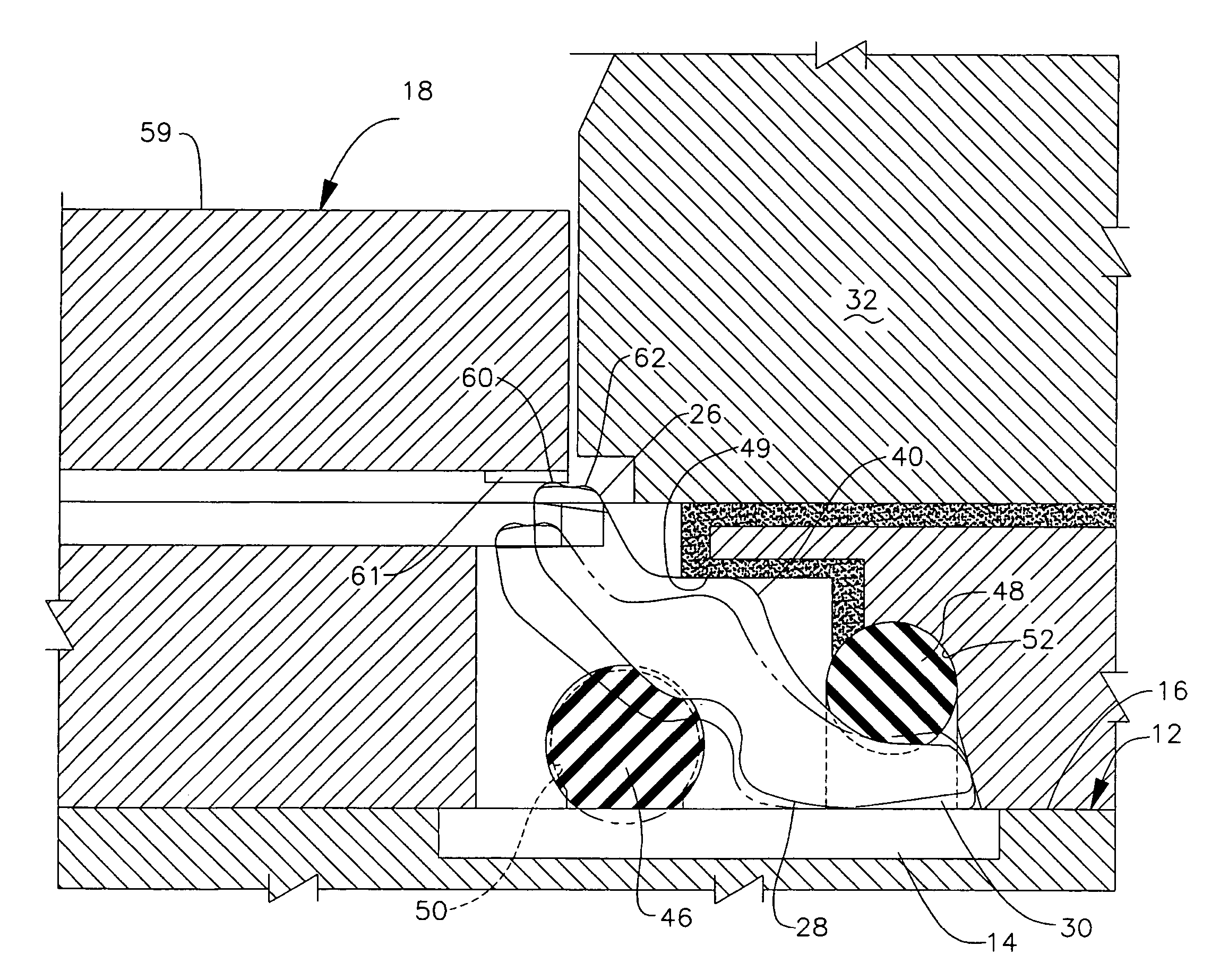
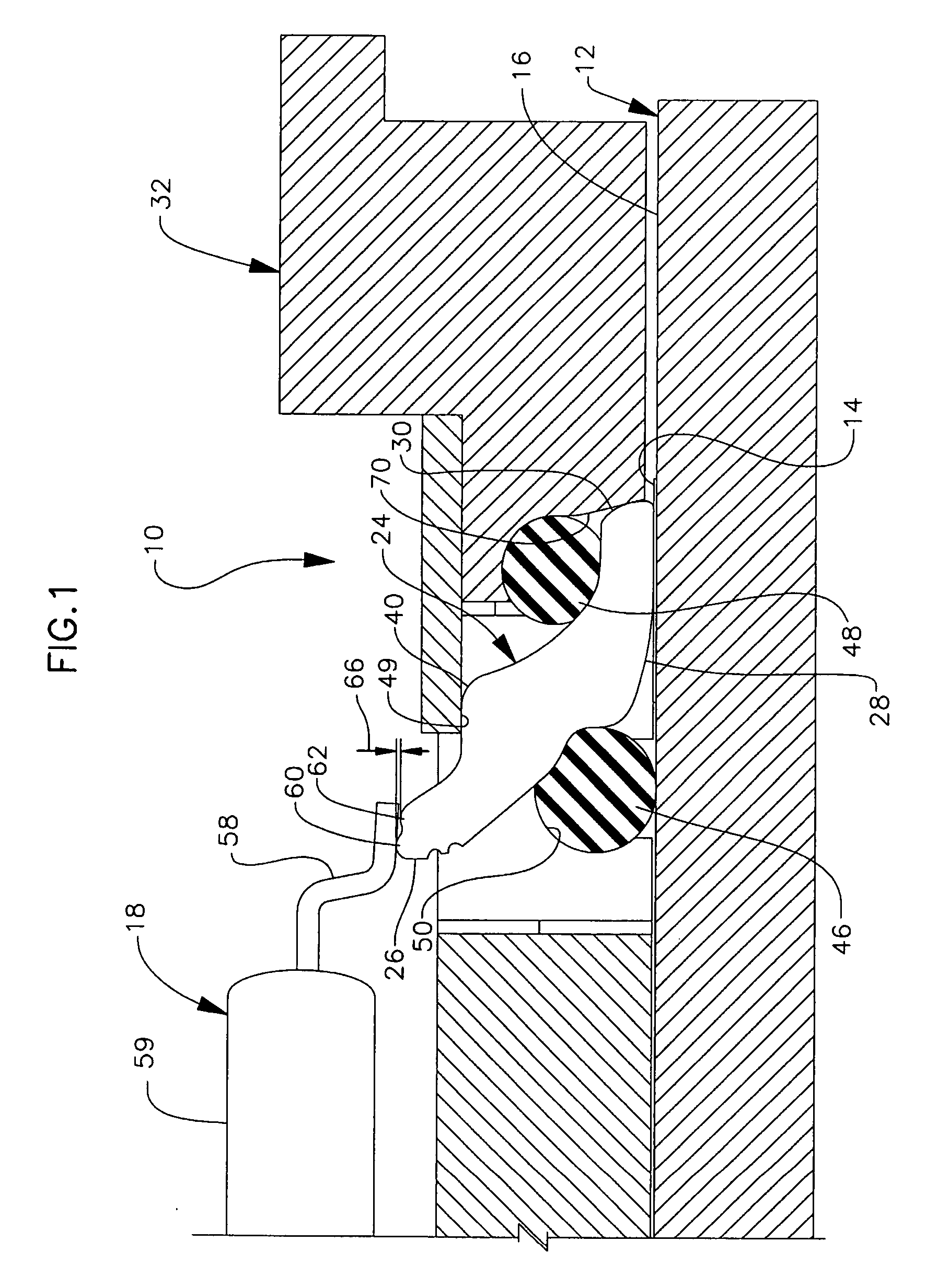
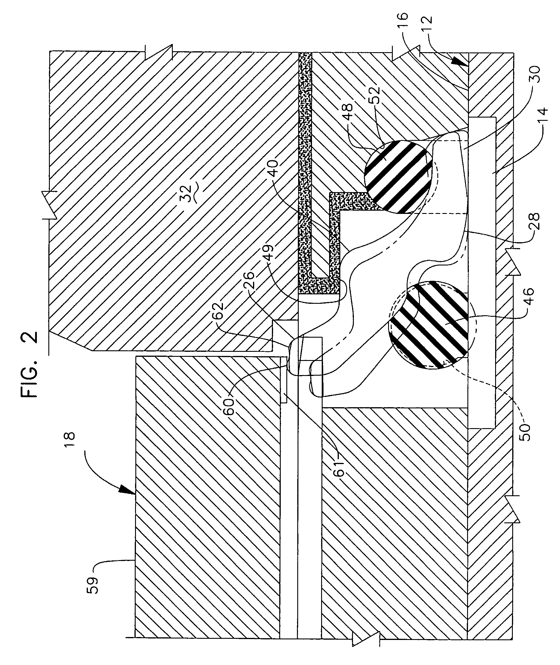
[0008] The present invention is a contact for use in a test set mountable to a load board of a tester apparatus. The contact serves to electrically connect at least one lead of a device to be tested (DUT) with a corresponding metallic trace on the load board. The contact has a first end which defines multiple contact points engageable by the lead of the DUT. It further has a second end having an arcuate edge in engagement with the metallic trace. The arcuate edge enables rolling across the metallic trace when the first end of the contact is engaged by the lead of the DUT and made to rotate about an axis generally perpendicular to a plane defined by the contact. The contact is elastomerically mounted as part of the test set intermediate the load board and the DUT. Rotation of the contact about the axis when the first end of the contact is engaged by the lead of the DUT is thereby facilitated.

Problems solved by technology

Further, it has been recognized that excessive wiping action can damage component parts at the various points of engagement of the contact, and thereby significantly decrease the life of the test socket and tester load board.
Another problem which has been discovered is the diminishment of effectiveness of testing as a result of the employment of matte tin on leads and pads of various types of DUTs.

Method used


Image

  • Electronic device test set and contact used therein
  • Electronic device test set and contact used therein
  • Electronic device test set and contact used therein

Examples


Embodiment Construction

[0016] Referring now to the drawing figures, wherein like reference numerals denote like elements throughout the several views, FIG. 1 illustrates a test socket 10 in accordance with the present invention. The test socket 10 is intended for use with a tester typically employed for ascertaining quality of integrated circuit devices used in electronic appliances. The tester interfaces with a tester load board 12 which has electrically conductive traces 14 formed on a surface 16 thereof to enable electronic communication between the tester and an integrated circuit device 18 to be tested. That is, electrical signals are transmitted between the device under test 18 and the test apparatus through the test socket 10.

[0017] It will be understood that various types of integrated circuit devices 18 are able to be tested utilizing a test socket or test set in accordance with the present invention. FIG. 1 illustrates a leaded device having externally-extending leads 58 diverging from the body...


PUM


Abstract

A contact for use in a test set which can be mounted to a load board of a tester apparatus. The contact, which serves to electrically connect at least one lead of a device being tested with a corresponding metallic trace on the load board, has a first end defining multiple contact points. As the contact is rotated about an axis generally perpendicular to a plane defined by the contact, successive contact points are sequentially engaged by a lead of the device being tested.

Description

CROSS-REFERENCE TO RELATED APPLICATIONS [0001] This is a regular application filed under 35 U.S.C. § 111(a) claiming priority, under 35 U.S.C. § 119(e) (1), of provisional application Ser. No. 60 / 776,654, previously filed Feb. 24, 2006 under 35 U.S.C. § 111(b).TECHNICAL FIELD [0002] The present invention relates broadly to the field of testing of electronic devices such as integrated circuits. More narrowly, however, the invention deals with test sets for interfacing pads or leads of a device to be tested with corresponding pads of a circuit board of a test apparatus. A specific embodiment of the invention focuses upon the construction and mounting of a contact of the test set. BACKGROUND OF THE INVENTION [0003] The testing of integrated circuit devices is performed to ensure that such devices, when sold to a customer, are of as high a degree of quality as possible. Various types of test apparatus have been utilized over the years to accomplish testing. Typically, a tester includes ...

Claims


Application Information

Patent Timeline
IPC IPC(8): G01R31/02
CPCG01R1/0466H01L22/00
Inventor SHELL, DENNIS B.GILK, MATHEW L.LOPEZ, JOSE E.
Owner JOHNSTECH INT
Learn More