Solid state imaging device

a solid-state imaging and imaging device technology, applied in the direction of radiation control devices, printers, instruments, etc., can solve the problems of affecting the reliability affecting the user's experience of the solid-state imaging device, so as to alleviate the user's uneasy sensation, and reduce the uneasy sensation of the user

Inactive Publication Date: 2007-10-11
RENESAS ELECTRONICS CORP
View PDF13 Cites 22 Cited by
  • Summary
  • Abstract
  • Description
  • Claims
  • Application Information

AI Technical Summary

Benefits of technology

[0009]In the solid-state imaging device thus constructed, the contact surface is a rough surface. Accordingly, after the object to be imaged, specifically a finger, is brought into direct contact with the contact surface, the residual fingerprint barely remains on the contact surface, unlike in the case where the contact surface is smooth. Also, the rough surface of the contact surface makes it difficult to recognize the residual fingerprint with naked eyes, thereby alleviating the uneasy sensation of the user.
[0010]Further, performing a surface treatment process, such as mechanical polishing, for roughening the contact surface incurs distortion on the contact surface due to the mechanical processing, which may offer an extrinsic gettering (hereinafter, EG) effect of capturing a metal or the like. The EG effect may, for example, prevent the impurity stuck to the finger from diffusing the semiconductor substrate, and from thereby degrading performance of a light receiving portion and MOSFET provided on the opposite side. The rough surface prevents, therefore, the degradation in reliability of the solid-state imaging device.
[0011]Thus, the present invention provides a solid-state imaging device that alleviates uneasy sensation of the user. Also, performing a surface treatment process, such as mechanical polishing, for making the contact surface rough enables preventing the impurity stuck to the finger from diffusing the semiconductor substrate, and from thereby degrading performance of a light receiving portion and MOSFET provided on the opposite side.

Problems solved by technology

Presence of such residual fingerprint which is visible with naked eyes provokes an uneasy sensation in the user of the solid-state imaging device, based on the fear that his / her fingerprint might be illegitimately acquired.
This leads to degraded reliability of the solid-state imaging device.
Also, the rough surface of the contact surface makes it difficult to recognize the residual fingerprint with naked eyes, thereby alleviating the uneasy sensation of the user.
Further, performing a surface treatment process, such as mechanical polishing, for roughening the contact surface incurs distortion on the contact surface due to the mechanical processing, which may offer an extrinsic gettering (hereinafter, EG) effect of capturing a metal or the like.

Method used


Image

  • Solid state imaging device
  • Solid state imaging device
  • Solid state imaging device

Examples


Embodiment Construction

[0017]The invention will be now described herein with reference to illustrative embodiments. Those skilled in the art will recognize that many alternative embodiments can be accomplished using the teachings of the present invention and that the invention is not limited to the embodiments illustrated for explanatory purposes.

[0018]Hereunder, an exemplary embodiment of a solid-state imaging device according to the present invention will be described in details, referring to the accompanying drawings. In the drawings, same constituents are given the same numerals, and the description thereof will not be repeated.

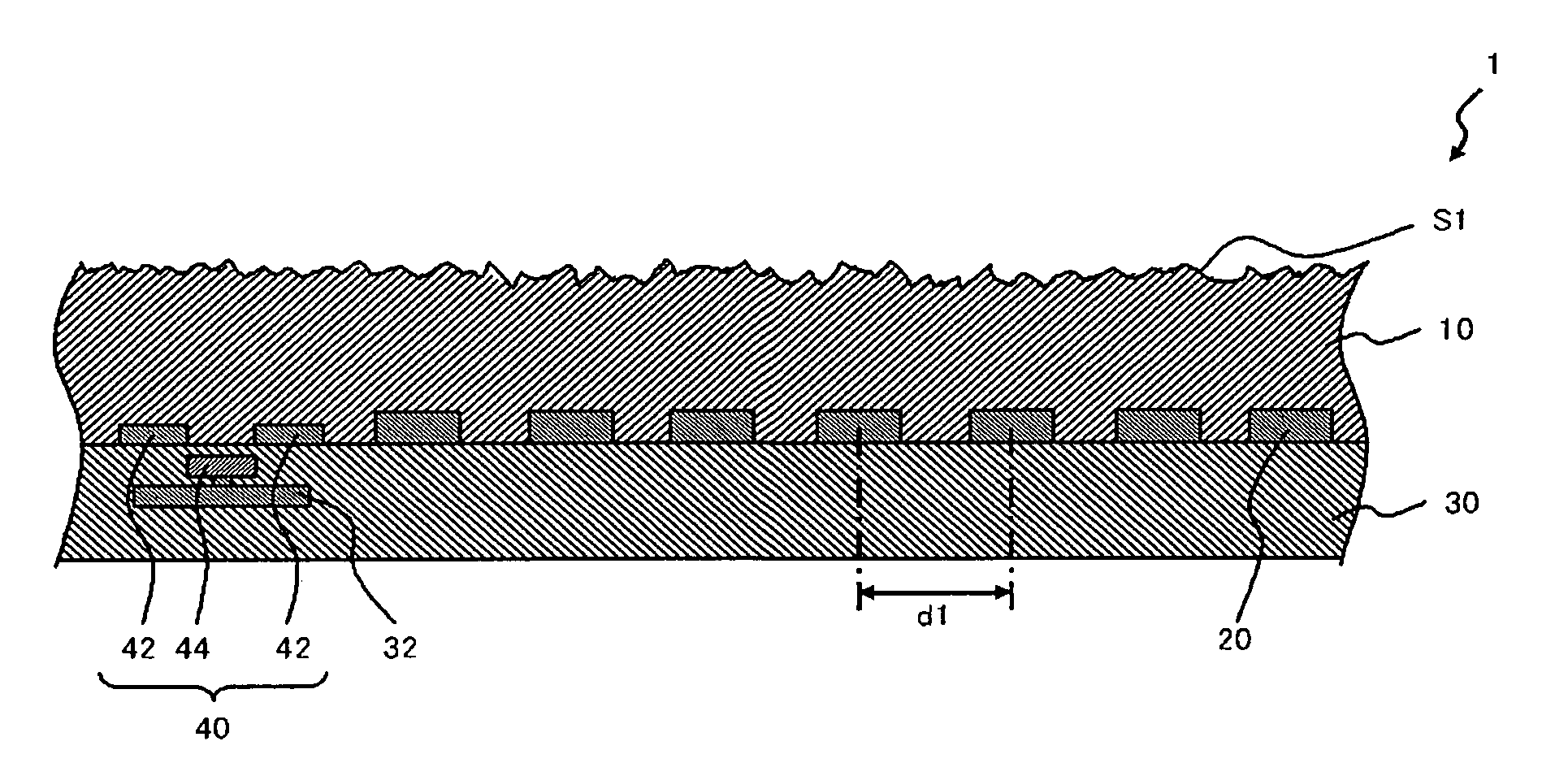
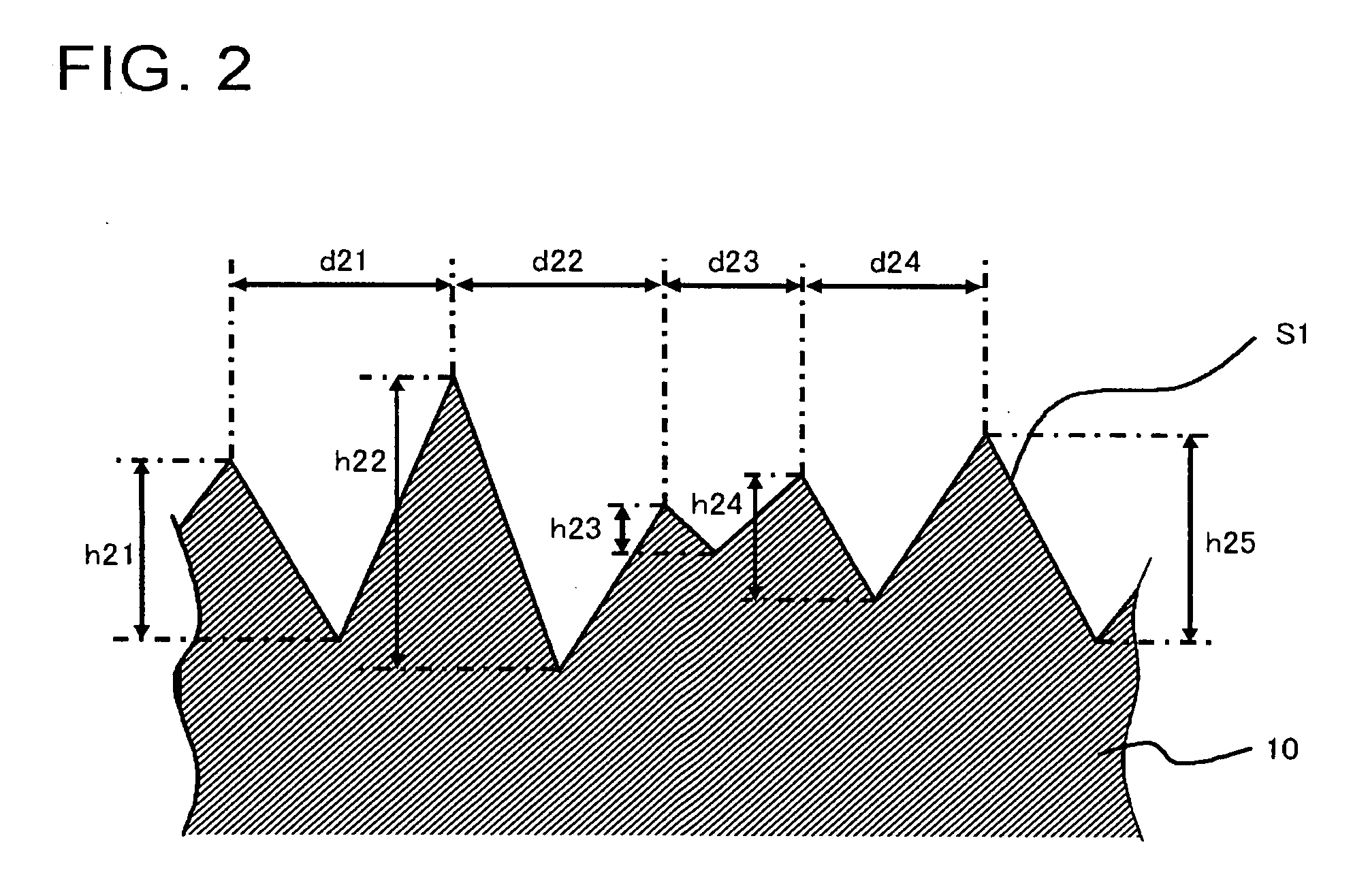
[0019]FIG. 1 is a cross-sectional view of a solid-state imaging device according to an embodiment of the present invention. The solid-state imaging device 1 includes a semiconductor substrate 10 and a light receiving portion 20. In this embodiment, the semiconductor substrate 10 is a P-type silicon substrate. On the back surface of the semiconductor substrate 10 (opposite to an...


PUM


Abstract

The solid-state imaging device includes a semiconductor substrate and a light receiving portion. On the back surface of the semiconductor substrate a contact surface is provided. The solid-state imaging device photoelectrically converts, in the semiconductor substrate, light transmitted through the object to be imaged in contact with the contact surface, and receives the electric charge generated by the photoelectric conversion with the light receiving portion, to thereby acquire the image of the object to be imaged. The contact surface is a rough surface.

Description

[0001]This application is based on Japanese patent application No. 2006-108304, the content of which is incorporated hereinto by reference.BACKGROUND[0002]1. Technical Field[0003]The present invention relates to a solid-state imaging device, and more particularly to a solid-state imaging device used for imaging a fingerprint.[0004]2. Related Art[0005]Conventional solid-state imaging devices applicable to imaging a fingerprint can be found, for example, in Japanese Laid-open patent publications No. 2004-246586 (patent document 1), No. 2002-33469 (patent document 2), No. 2000-217803 (patent document 3), and No. 2002-74345 (patent document 4). The solid-state imaging devices disclosed in these documents include a contact surface on which a finger is to be placed, for shooting an image of the fingerprint of the finger placed on the contact surface.[0006]In addition to the documents cited above, prior art literature relevant to the present invention includes Japanese Laid-open patent pub...

Claims


Application Information

Patent Timeline
Patent Type & Authority Applications(United States)
IPC IPC(8): G03B29/00H01L27/146H01L31/10H04N5/335H04N5/369
CPCG03B29/00
Inventor NAKASHIBA, YASUTAKA
Owner RENESAS ELECTRONICS CORP
Why Eureka
Try Eureka