Light emitting diode package and fabrication method thereof

a technology of light-emitting diodes and fabrication methods, which is applied in the direction of basic electric elements, electrical equipment, semiconductor devices, etc., can solve the problems of increasing manufacturing time and cost, low heat radiation efficiency, and complicated conventional heat radiation structure, and achieves superior heat radiation efficiency and simple configuration

Inactive Publication Date: 2007-10-18
SAMSUNG ELECTRONICS CO LTD
View PDF10 Cites 114 Cited by
  • Summary
  • Abstract
  • Description
  • Claims
  • Application Information

AI Technical Summary

Benefits of technology

[0015]The present invention has been made to solve the foregoing problems of the prior art and therefore an aspect of the pre

Problems solved by technology

However, this conventional heat radiation structure is complicated and requires many components.
Therefore, it is difficult to automate the manufacturing process of the LED package with assembly of many components, thus increasing

Method used


Image

  • Light emitting diode package and fabrication method thereof
  • Light emitting diode package and fabrication method thereof
  • Light emitting diode package and fabrication method thereof

Examples


Embodiment Construction

[0051]Exemplary embodiments of the present invention will now be described in detail with reference to the accompanying drawings.

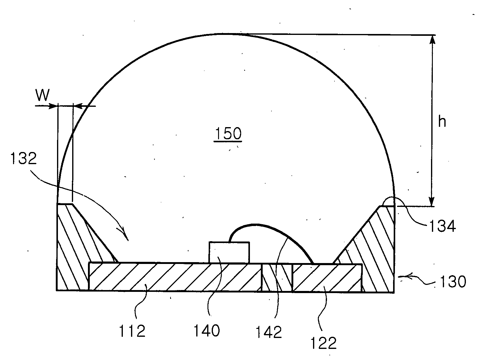
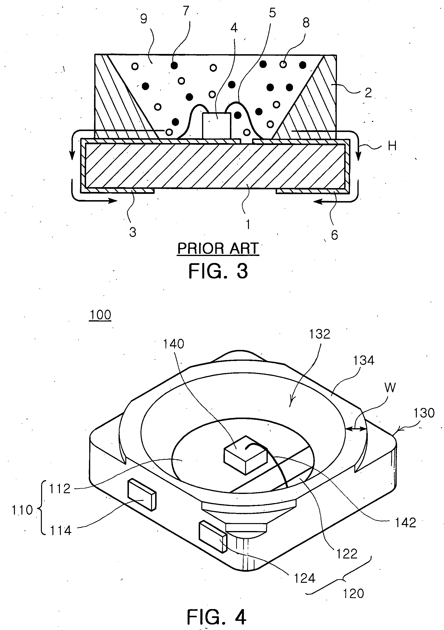
[0052]An LED package according to a first embodiment of the present invention is illustrated in FIGS. 4 to 8.

[0053]The LED package 100 according to this embodiment includes a pair of metal lead frames 110 and 120 and an insular package body 130 surrounding the lead frames 110 and 120.

[0054]The first lead frame 110 includes a planar base 112 and a pair of extensions 114 extending from opposed ends of the base 112. It is preferable that the base 112 is provided in an area as large as possible so that it has a large contact area as possible with a circuit board (see FIG. 10) described later, which is a heat sink. The extensions 114 are formed in a smaller width than the base 112, and are surrounded by the package body 130 to secure the lead frame 110 to the package body 130. Of course, the extensions 114 can be formed in the same width as the base 112, which ...


PUM


Abstract

An LED package and a fabrication method therefor. The LED package includes first and second lead frames made of heat and electric conductors, each of the lead frames comprising a planar base and extensions extending in opposed directions and upward directions from the base. The package also includes a package body made of a resin and configured to surround the extensions of the first and second lead frames to fix the first and second lead frames while exposing underside surfaces of the first and second lead frames. The LED package further includes a light emitting diode chip disposed on an upper surface of the base of the first lead frame and electrically connected to the bases of the first and second lead frames, and a transparent encapsulant for encapsulating the light emitting diode chip.

Description

CLAIM OF PRIORITY[0001]This application claims the benefit of Korean Patent Application No. 2006-0034706 filed on Apr. 17, 2006, in the Korean Intellectual Property Office, the disclosure of which is incorporated herein by reference.BACKGROUND OF THE INVENTION[0002]1. Field of the Invention[0003]The present invention relates to a Light Emitting Diode (LED) and, more particularly, to an LED package having a simple configuration with superior heat radiation efficiency, and a fabrication method thereof.[0004]2. Description of the Related Art[0005]A light emitting diode (LED) is a semiconductor device for generating various colors of light in response to current application. The colors generated from the LED are determined by the chemical substances constituting the semiconductor of the LED. Such an LED has various merits such as a long lifetime, low power, excellent initial driving characteristics, high resistance for vibration and high tolerance for frequent power on / off compared to a...

Claims


Application Information

Patent Timeline
IPC IPC(8): H01L33/00H01L33/60H01L33/52H01L33/62H01L33/64
CPCH01L33/486H01L33/62H01L33/642H01L33/647H01L2224/48247H01L2224/48091H01L2924/00014
Inventor HAN, KYUNG TAEGYEO, IN TAEHAHM, HUN JOOSONG, CHANG HOHAN, SEONG YEONNA, YOON SUNGKIM, DAE YEONAHN, HO SIKPARK, YOUNG SAM
Owner SAMSUNG ELECTRONICS CO LTD
Why Eureka
Try Eureka