Stacked semiconductor device and fabrication method for same

a technology of semiconductor devices and fabrication methods, which is applied in the direction of semiconductor devices, semiconductor/solid-state device details, electrical apparatus, etc., can solve the problems of increasing the height of the package, increasing the height of the stacked semiconductor devices, so as to reduce the thickness of the protruding linking interconnects that protrude on the upper surface of the encapsulant, the effect of reducing the thickness of the protruding linking interconn

Active Publication Date: 2007-10-18
LONGITUDE LICENSING LTD
View PDF5 Cites 100 Cited by
  • Summary
  • Abstract
  • Description
  • Claims
  • Application Information

AI Technical Summary

Benefits of technology

[0100]In the lower semiconductor device, the portions of the linking interconnects that overlie the encapsulant are formed in trenches provided from the side surfaces and across the upper surface of the encapsulant. As a result, the height (thickness) of the protrusion of the linking interconnects that protrude on the upper surface of the encapsulant can be decreased compared to the case of the lower semiconductor device constructed by the means of the above-described “1.” In this way, a stacked semiconductor device of even thinner construction can be achieved.
[0101]A stacked semiconductor device constructed by the means of the above-described “3” has the following effects in addition to the effect constructed by the stacked semiconductor device of the above-described means (1).
[0102]In the lower semiconductor device, the portions of the linking interconnects that extend from the side surfaces of the encapsulant as far as the outer periphery of the wiring board are covered and protected by a protective layer composed of insulating plastic, whereby short-circuit defects that occur when extraneous matter adheres to the wiring and linking interconnects can be prevented. The reliability of the stacked semiconductor device can thus be increased.

Problems solved by technology

When semiconductor devices of this type are stacked, the peripheral portion of the wiring board is caused to protrude to expose a portion of the wiring outside of the encapsulant.
Arranging and stacking two levels of semiconductor chips on the package of the lower semiconductor device in this type of configuration increases the height of the package, and as a result, a bump electrode formed by one solder ball no longer has sufficient height.
However, in a stacked semiconductor device having this type of construction, the height of the stacked semiconductor devices increases and thus complicates the realization of thinner stacked semiconductor devices.
In addition, the need for the portion of the wiring board outside of the package for connecting bump electrodes further complicates the realization of smaller stacked semiconductor devices.

Method used


Image

  • Stacked semiconductor device and fabrication method for same
  • Stacked semiconductor device and fabrication method for same
  • Stacked semiconductor device and fabrication method for same

Examples


first embodiment

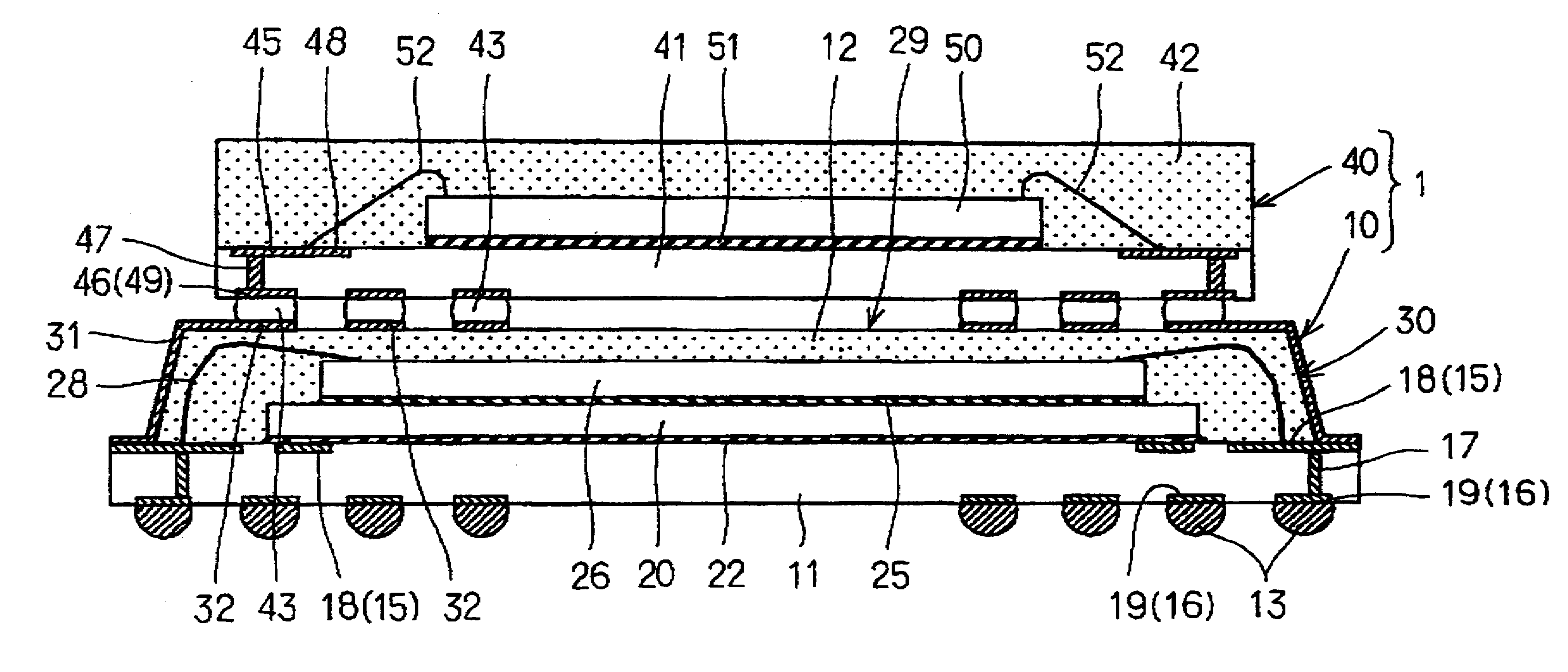
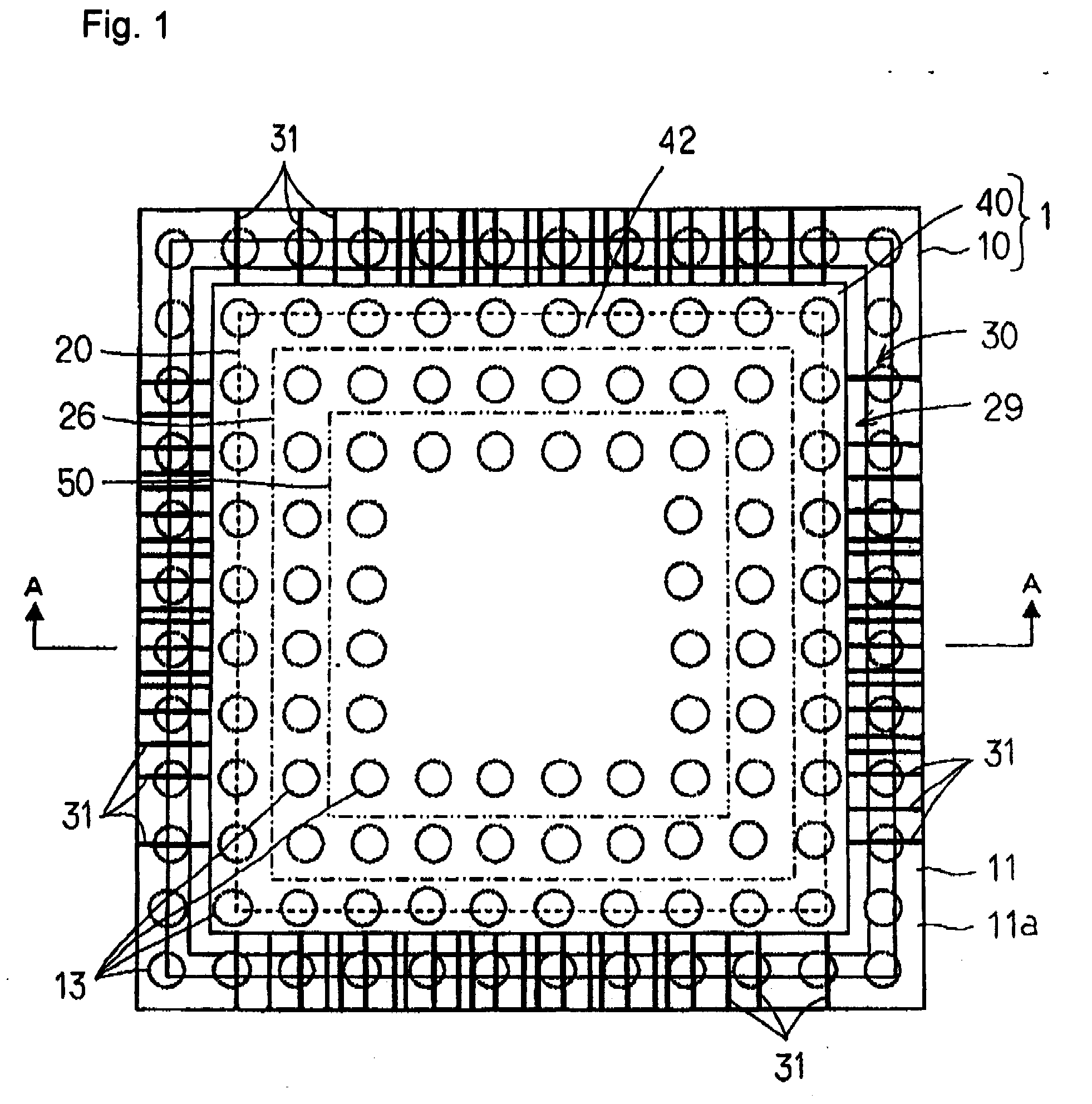
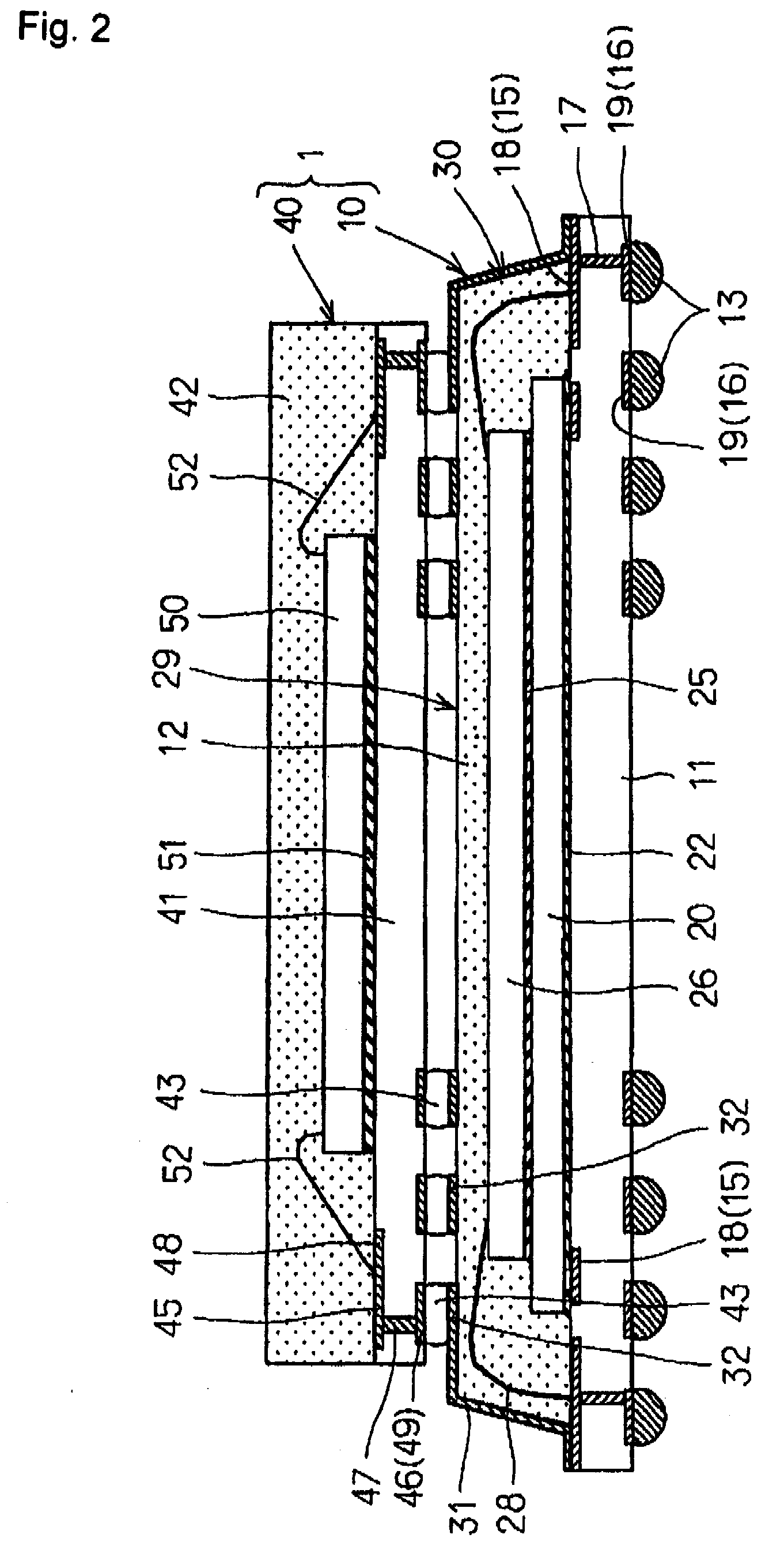
[0133]FIGS. 1 to 18 are figures relating to the stacked semiconductor device of the first embodiment of the present invention and to the fabrication method of this stacked semiconductor device. FIGS. 1 to 7 are figures relating to the construction of the stacked semiconductor device. FIGS. 8A, 8B, 8C, 8D, 8E, 8F to FIG. 18 are figures relating to the fabrication method of the semiconductor device.

[0134]The stacked semiconductor device of the present invention is a semiconductor device in which a plurality of semiconductor devices are stacked in multiple layers. In the first embodiment, explanation relates to a case in which the present invention is applied to a stacked semiconductor device in which two semiconductor devices are stacked.

[0135]As shown in FIGS. 1 and 2, stacked semiconductor device 1 of the first embodiment is made up of lower semiconductor device 10 and upper semiconductor device 40 that is stacked on this lower semiconductor device 10. Lower semiconductor device 10 ...

second embodiment

[0180]FIGS. 19 to 23 relate to the fabrication method of a stacked semiconductor device of the second embodiment of the present invention. The second embodiment relates to another method of forming linking interconnects 31 of lower semiconductor device 10 in the fabrication method of a stacked semiconductor device of the first embodiment. In other words, the portions of linking interconnects 31 that overlie encapsulant 12 are formed in trenches 81 provided from side surfaces 30 and across upper surface 29 of encapsulant 12. FIG. 19 shows trenches 81 provided from side surfaces 30 and across upper surface 29 of encapsulant 12, and FIG. 23 shows linking interconnects 31 that are embedded in trenches 81. The circular portions of upper surface 29 of encapsulant 12 serve as linking connection pads 32.

[0181]When fabricating lower semiconductor device 10 of this configuration, a mold die provided with protrusions corresponding to linking interconnects in the wall surface of the cavities th...

third embodiment

[0184]FIG. 24 is a plan view showing the first semiconductor device that has been fabricated by the fabrication method of a stacked semiconductor device of the third embodiment of the present invention. FIG. 25 is a sectional view taken along line D-D of FIG. 24.

[0185]As shown in FIG. 24 and FIG. 25, in lower semiconductor device 10 in the stacked semiconductor device of the third embodiment, protective layer 90 composed of insulating plastic covers the portions of linking interconnects 31 on the side of first surface 11a of wiring board 11 that extends from side surfaces 30 of encapsulant 12 and reaches the outer edges of wiring board 11 on lower semiconductor device 10 of the first embodiment.

[0186]In this lower semiconductor device 10, in the fabrication method of lower semiconductor device 10 of the first embodiment shown in FIGS. 10(a)-(c), protective layer 90 is formed after forming linking interconnects 31 as shown in FIG. 10(b) by embedding insulating plastic at the outer pe...


PUM


Abstract

A stacked semiconductor device is constructed by stacking in two levels: a lower semiconductor device having a wiring board, at least one semiconductor chip mounted on a first surface of the wiring board and having electrodes electrically connected to wiring by way of a connection means, an encapsulant composed of insulating plastic that covers the semiconductor chip and the connection means, a plurality of electrodes formed overlying the wiring of a second surface of the wiring board, and a plurality of linking interconnects each having a portion connected to the wiring of the first surface of the wiring board and another portion exposed on the surface of the encapsulant; and an upper semiconductor device in which each electrode overlies and is electrically connected to the exposed portions of each of the linking interconnects of the lower semiconductor device. The linking interconnects extend from the first surface of the wiring board to the side surfaces and upper surface of the encapsulant, and moreover, electrically connect with wiring of the wiring board that projects from the encapsulant.

Description

BACKGROUND OF THE INVENTION[0001]1. Field of the Invention[0002]The present invention relates to a semiconductor device and a method of fabricating the device. In particular, the present invention relates to a technology effective for application to the fabrication technology of stacked semiconductor devices in which a semiconductor device is stacked on the upper surface of a semiconductor device.[0003]2. Description of the Related Art[0004]Surface-mount semiconductor devices referred to as BGA (Ball Grid Array) constructions and LGA (Land Grid Array) are known in the art as package configurations for realizing semiconductor devices of greater integration as well as smaller size and lighter weight.[0005]In this type of semiconductor device, semiconductor elements (semiconductor chips) are affixed to a wiring board. In this type of semiconductor device, the electrodes of semiconductor chips and connection pads that are formed by the wiring of the wiring board are connected by conduct...

Claims


Application Information

Patent Timeline
Patent Type & Authority Applications(United States)
IPC IPC(8): H01L23/02
CPCH01L23/3128H01L2924/07802H01L25/0657H01L25/105H01L2224/32145H01L2224/48091H01L2224/48227H01L2224/48465H01L2224/48471H01L2224/73265H01L2224/97H01L2225/0651H01L2225/06517H01L2225/06551H01L2924/01013H01L2924/01029H01L2924/01047H01L2924/01082H01L2924/15311H01L2924/15331H01L24/97H01L2224/92247H01L2225/1058H01L2225/1023H01L2224/32225H01L2224/16225H01L2924/12041H01L2924/014H01L2924/01033H01L2924/01019H01L2924/01006H01L2924/01005H01L2224/85H01L2924/00014H01L2224/83H01L2924/00H01L2924/00012H01L2225/1041H01L2924/181H01L24/73H01L2224/81
Inventor KAGAYA, YUTAKATAKESHIMA, HIDEHIROISHIHARA, MASAMICHI
Owner LONGITUDE LICENSING LTD
Why Eureka
Try Eureka