Resin molded semiconductor device and method for manufacturing the same

a semiconductor device and resin technology, applied in semiconductor devices, semiconductor/solid-state device details, electrical devices, etc., can solve problems such as serious quality control problems, such as impurity deposition, and inability to efficiently mount,

Inactive Publication Date: 2001-09-18
PANASONIC CORP
View PDF18 Cites 63 Cited by
  • Summary
  • Abstract
  • Description
  • Claims
  • Application Information

AI Technical Summary

Benefits of technology

According to this method, it is possible to form easily a resin-molded semiconductor device, which a solid-state imaging device or the like, requiring an overlying...

Problems solved by technology

Accordingly, mounting cannot be carried out efficiently.
Even so, there occurs a problem that the resin encapsulant reaches the back surface of the inner leads to form a resin bur (overflowing resin) on the surface of the external electrodes.
However, such a water jet process step is very troublesome and is contradictory to the demand on a process simplification to manufacture resin-molded semiconductor devices in high volume or on a reduction in number of process steps.
In the conventional process, however, if the resin bur is blown off with high-pressure water jet during the water jet process step introduced to remove the re...

Method used


Image

  • Resin molded semiconductor device and method for manufacturing the same
  • Resin molded semiconductor device and method for manufacturing the same
  • Resin molded semiconductor device and method for manufacturing the same

Examples


first embodiment

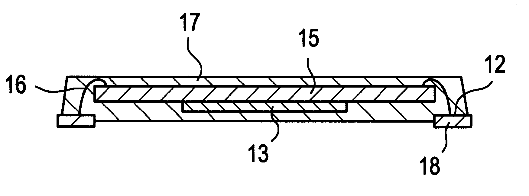
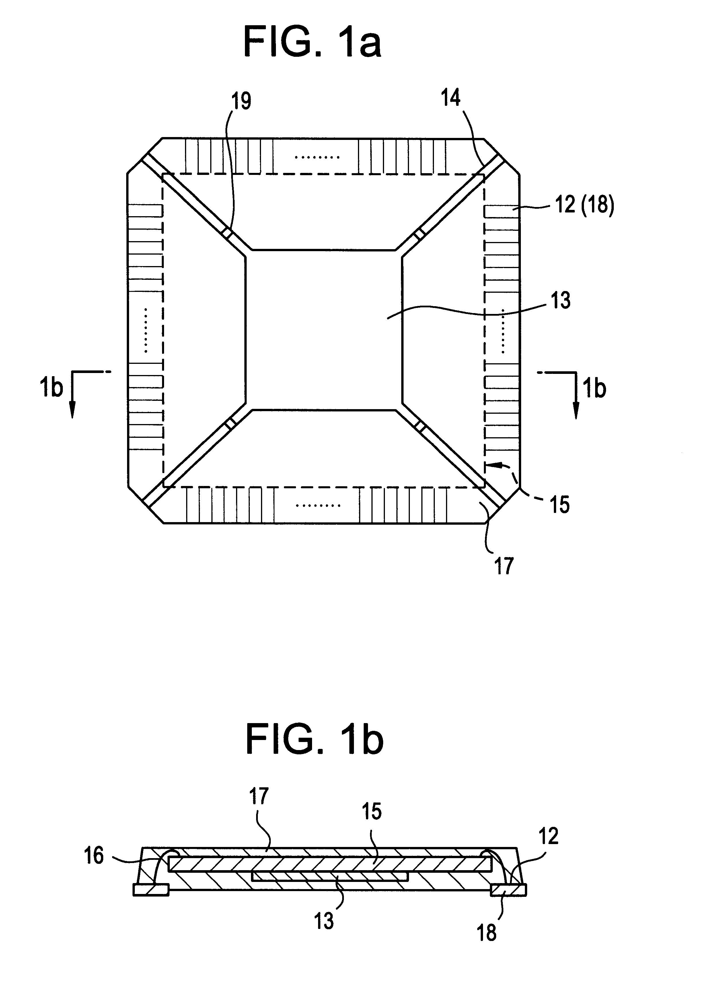
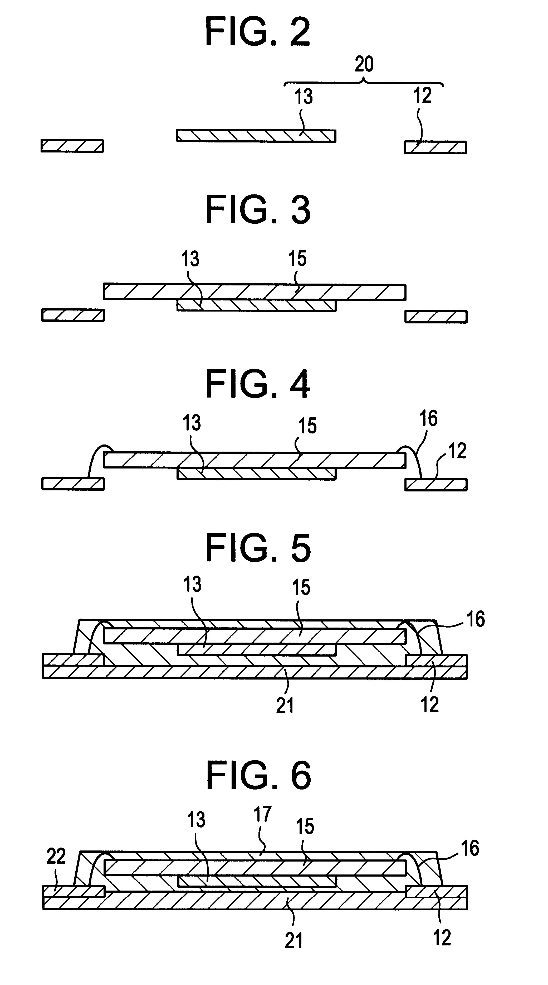
FIG. 1(a) is a plan view of a resin-molded semiconductor device and FIG. 1(b) is a cross-sectional view thereof taken along the line 1b--1b in FIG. 1(a). In FIG. 1(a), a resin encapsulant 17 is illustrated as being transparent, a semiconductor chip 15 has a contour as indicated by the dashed line, and the illustration of metal fine wires 16 is omitted.

As shown in FIGS. 1(a) and 1(b), the resin-molded semiconductor device of this embodiment includes a leadframe consisting of: inner leads 12; a die pad 13 for supporting the semiconductor chip thereon; and support leads 14 for supporting the die pad 13. The semiconductor chip 15 is bonded on the die pad 13 with an adhesive, and electrode pads (not shown) of the semiconductor chip 15 are electrically connected to the inner leads 12 with metal fine wires 16. And the inner leads 12, die pad 13, support leads 14, semiconductor chip 15 and metal fine wires 16 are encapsulated within the resin encapsulant 17. Also, the die pad 13 is elevate...

embodiment 2

Next, a second embodiment of the present invention will be described. FIG. 9 is a cross-sectional view illustrating a resin-molded semiconductor device of a substrate-bonded type according to this embodiment.

As shown in FIG. 9, the resin-molded semiconductor device of this embodiment is of a substrate-bonded type such as a BGA (ball grid array) type. The device includes: a substrate 24 made of single- or multiple-layered glass epoxy plastic or ceramic; a semiconductor chip 25 mounted on the substrate 24; and metal fine wires 26 for electrically connecting interconnects (not shown) formed on the upper surface of the substrate 24 to electrode pads (not shown) of the semiconductor chip 25. And over the upper surface of the substrate 24, the semiconductor chip 25, interconnects and metal fine wires 26 are molded with an insulating resin encapsulant 27. On the back of the substrate 24, external electrode pads (lands) 28 are formed. The interconnects on the upper surface of the substrate ...

embodiment 3

Next, a third embodiment of the present invention will be described. FIG. 13 is a cross-sectional view illustrating a resin-molded semiconductor device according to this embodiment. The resin-molded semiconductor device of this embodiment includes: a radiator plate; and a semiconductor chip incorporating a device generating a relatively large quantity of heat, e.g., a high-power transistor.

As shown in FIG. 13, the semiconductor device of this embodiment includes: a bed 33, or a support for a leadframe; a semiconductor chip 34 bonded on the bed 33 with a die-bonding member; a metal terminal 35 of the leadframe; a metal fine wire 36 for electrically connecting the metal terminal 35 to the semiconductor chip 34; and a radiator plate 37 for supporting the bed 33 thereon. In this structure, all the members are entirely molded with an insulating resin encapsulant 38, except for the bottom of the radiator plate 37 and part of the metal terminal 35 protruding out of the resin encapsulant 38...


PUM


Abstract

A method for manufacturing a semiconductor chip (15) which is bonded on a die pad (13) of a leadframe, and inner leads (12) are electrically connected to electrode pads of the semiconductor chip (15) with metal fine wires (16). The die pad (13), semiconductor chip (15) and inner leads are molded with a resin encapsulant (17). However, no resin encapsulant (17) exists on the respective back surfaces of the inner leads (12), which protrude downward from the back surface of the resin encapsulant (17) so as to be external electrodes (18).

Description

The present invention relates to a resin-molded semiconductor device, in which a semiconductor chip and a leadframe are molded with a resin encapsulant, and to a method for manufacturing such a device. In particular, the present invention relates to a device with the back surface of the leadframe partially exposed out of the resin encapsulant.In recent years, in order to catch up with rapidly advancing downsizing of electronic units, it has become increasingly necessary to package semiconductor components for each of these electronic units at a higher and higher density. Correspondingly, sizes and thicknesses of semiconductor components have also been noticeably reduced.Hereinafter, a conventional resin-molded semiconductor device will be described.FIG. 23(a) is a plan view of a conventional resin-molded semiconductor device, and FIG. 23(b) is a cross-sectional view of the conventional resin-molded semiconductor device.As shown in FIGS. 23(a) and 23(b), this conventional resin-molde...

Claims


Application Information

Patent Timeline
IPC IPC(8): H01L21/67H01L21/56H01L23/31H01L23/28H01L23/495H01L21/68H01L23/48H01L21/02
CPCH01L21/565H01L21/566H01L21/568H01L23/3107H01L23/49503H01L2924/3025H01L2924/12041H01L2224/48227H01L2224/16225H01L2924/01028H01L2924/01013H01L2924/01322H01L24/48H01L2924/16195H01L24/45H01L2224/16H01L2224/32014H01L2224/45124H01L2224/45144H01L2224/48091H01L2224/48247H01L2924/01004H01L2924/01046H01L2924/0105H01L2924/01078H01L2924/01079H01L2924/09701H01L2924/14H01L2924/15153H01L2924/15165H01L2924/15311H01L2924/00014H01L2924/00H01L2924/181H01L2924/00012H01L21/56H01L23/28
Inventor OIDA, SEISHIYAMAGUCHI, YUKIOSUEMATSU, NOBUHIRO
Owner PANASONIC CORP
Why Eureka
Try Eureka