Systems for displaying images involving reduced mura

a mura and image technology, applied in the field of display devices, can solve the problems of poor display uniformity of prior art amoled b>10/b>

Active Publication Date: 2007-10-18
INNOLUX CORP
View PDF4 Cites 183 Cited by
  • Summary
  • Abstract
  • Description
  • Claims
  • Application Information

AI Technical Summary

Benefits of technology

[0023] Another exemplary embodiment of such as system comprises a pixel, a data line and a scan reset line. The pixel has a driving TFT, with the driving TFT being operative to control illumination of the pixel. The data line is operative to provide display signals and sweep signals to the pixel. The scan reset line is operative to provide scan reset signals to the pixel. The driving TFT has a linear region and a saturation region, and the driving TFT exhibits an operating point within the linear region.

Problems solved by technology

Therefore, the prior art AMOLED 10 has poor display uniformity even with slight variation of TFT characteristics.

Method used


Image

  • Systems for displaying images involving reduced mura
  • Systems for displaying images involving reduced mura
  • Systems for displaying images involving reduced mura

Examples


first embodiment

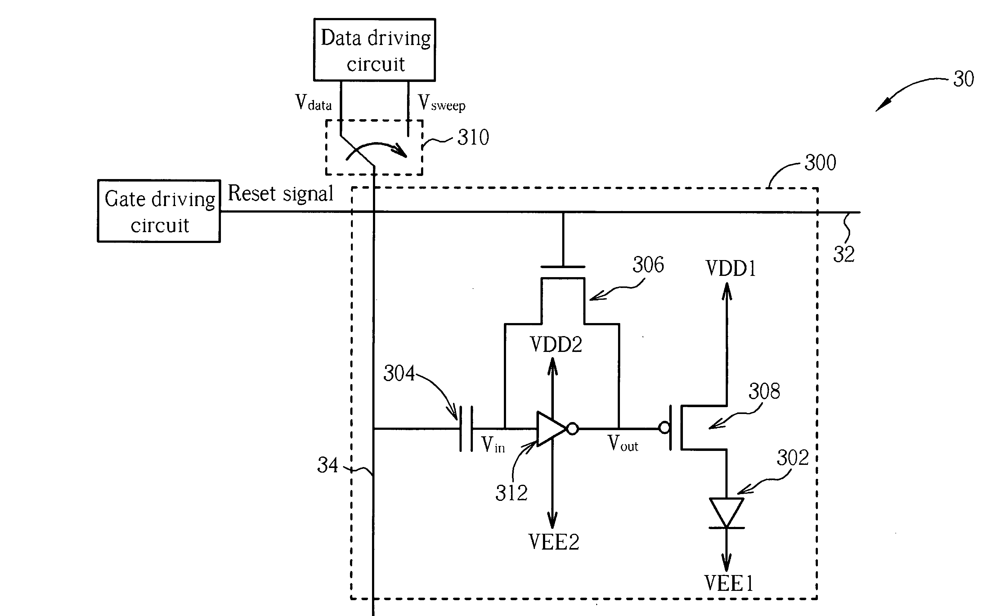
[0040]FIG. 5 shows the matrix of the AMOLED 30 according to the present invention. The AMOLED 30 shown in FIG. 5 includes a data driving circuit 36, a gate driving circuit 38, a plurality of data lines 34, a plurality of scan reset lines 32, and a plurality of pixels 300. Power lines 51-54 are used to respectively provide power from the voltage sources VDD1, VDD2, VEE1 and VEE2 to each pixel 300. The voltage source VDD1 supplies voltages to the pixels 300 via corresponding switches 410. The relay switches 310 control passages of the data signal Vdata and the sweep signal Vsweep from the data driving circuit 36 into corresponding data lines 34.

[0041]FIG. 6 shows a timing diagram illustrating the overall operation of the first embodiment during a frame period. Vout represents the voltage level at the output end of the inversion unit 312, and Vsweep represents the voltage level of a sweep signal. Normally, a triangular pixel driving voltage as shown in FIG. 6 is used for the sweep sign...

second embodiment

[0046]FIG. 8 shows a system for displaying images that includes an AMOLED 60. The AMOLED 60 includes a plurality of pixels 600 arranged in a matrix manner, and only one pixel is shown in FIG. 6 for simplicity. The AMOLED 60 differs from the AMOLED 30 in that the AMOLED 60 includes a plurality of storage capacitors 304, reset switches 306, and inversion units 312. The inversion units 312 are coupled in series between the data line 34 and the gate of the driving TFT 308. The voltages established at the input and output ends of the series-coupled inversion units 312 are designated as Vin and Vout, respectively. The voltage sources used in the AMOLED 60 has the following relationship VDD2≧VDD1>VEE1≧VEE2, so that the driving TFT 308 works in the linear region.

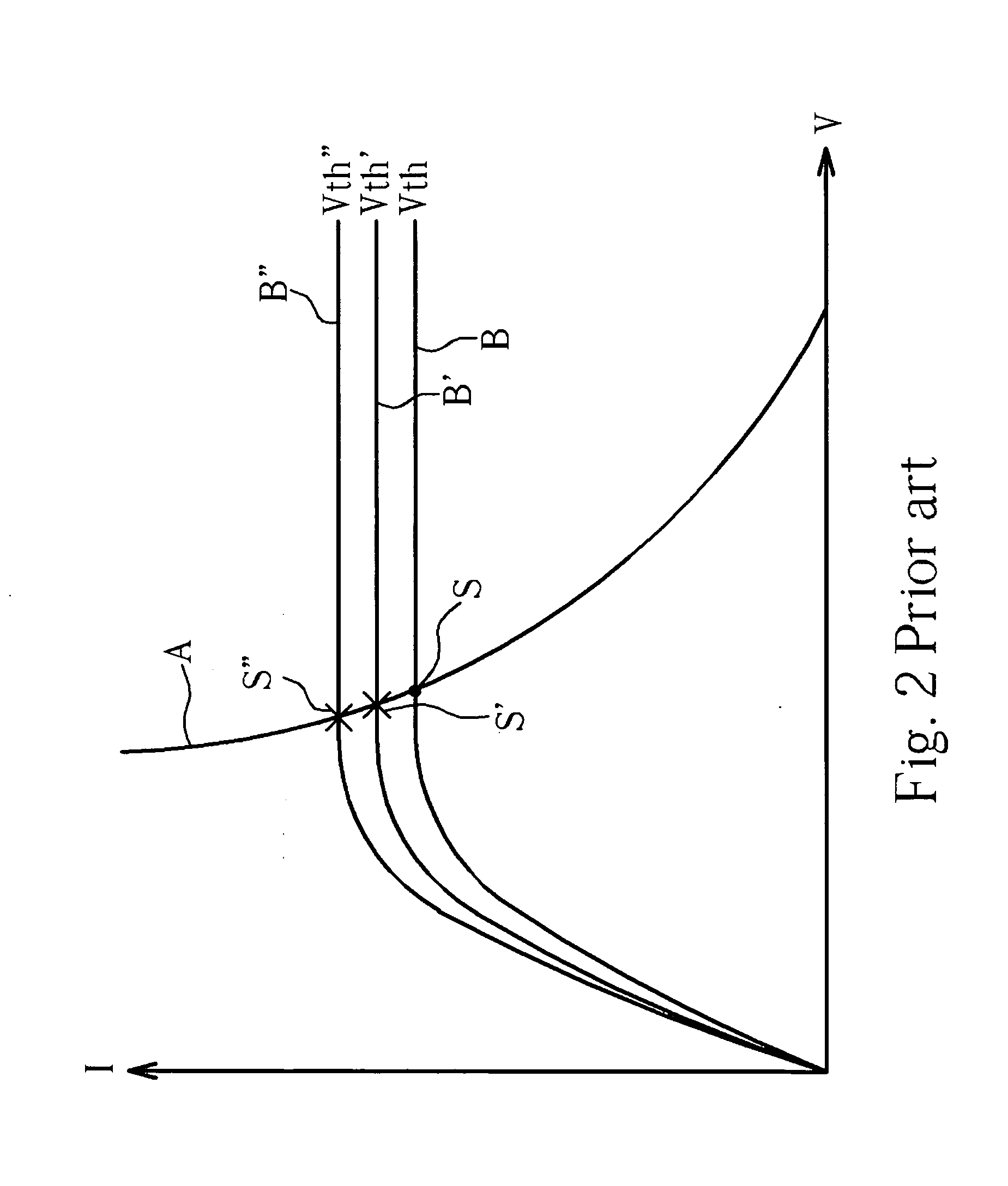
[0047]FIG. 9 shows an overall Vin-Vout characteristic of the series-coupled inversion units 312 in AMOLED 80. In FIG. 9, a solid curve represents the voltage characteristic, Vto′ represents a turn-on voltage of the driving TFT 308 o...

third embodiment

[0048]FIG. 10 shows a system for displaying images that includes an AMOLED 70. The AMOLED 70 includes a plurality of pixels 700 arranged in a matrix manner, and only one pixel is shown in FIG. 7 for simplicity. The pixels 700, each including an OLED 702 as a pixel light emitting device, are coupled to external driving circuits via a corresponding scan line 72, a data line 74 and a sweep line 76. Each pixel 700 further includes a storage capacitor 704, a control switch 706, a driving TFT 708, a relay switch 710 and an inversion unit 712. The control switch 706, coupled between an input end of the inversion unit 712 and the data line 74, is either turned on or turned off based on scan signals received from the scan line 72. The storage capacitor 704, coupled between the sweep line 76 and the input end of the inversion unit 712, stores charges of sweep signals Vsweep via the relay switch 710. The driving TFT 708 can include a p-type TFT having a gate coupled to an output end of the inv...


PUM


Abstract

Systems for displaying images are provided. A representative system incorporates a display device that includes a data line operative to provide display signals and sweep signals; a scan line operative to provide scan reset signals; a first capacitor having a first end coupled to the data line for storing charges from the signal line; a first inversion unit having an input end coupled to a second end of the first capacitor, a first supply end coupled to a first voltage source, a second supply end coupled to a second voltage source larger than the first voltage, and an output end; a first reset switch having a first end coupled between the second end of the first capacitor and the input end of the first inversion unit, a second end coupled to the output end of the first inversion unit, and a control end coupled to the scan line; a driving TFT having a control end coupled to the output end of the first inversion unit; and an illuminating unit coupled between a first end of the driving TFT and a third voltage source larger than or equal to the first voltage source.

Description

BACKGROUND OF THE INVENTION [0001] 1. Field of the Invention [0002] The present invention relates to display devices. [0003] 2. Description of the Prior Art [0004] With rapid development of planar displays, more and more planar display technologies are being researched for increasing product competitiveness. In order to meet the needs of demanding applications, the flat panel industry is now looking at displays known as active-matrix organic light emitting displays (AMOLEDs). An AMOLED has an integrated electronic back plane as its substrate and is particularly suitable for high-resolution, high-information content applications including videos and graphics. This form of display is made possible by the development of polysilicon technology, which, because of its high carrier mobility, provides thin-film-transistors (TFTs) with high current carrying capability and high switching speed. In an AMOLED display, each individual pixel can be addressed independently via the associated drivi...

Claims


Application Information

Patent Timeline
Patent Type & Authority Applications(United States)
IPC IPC(8): G09G3/30
CPCG09G3/2014G09G3/3258G09G3/3291G09G2300/0819G09G2320/043G09G2300/0852G09G2300/0861G09G2310/0251G09G2300/0842
Inventor LIN, CHING-WEI
Owner INNOLUX CORP
Why Eureka
Try Eureka