Image display device
- Summary
- Abstract
- Description
- Claims
- Application Information
AI Technical Summary
Benefits of technology
Problems solved by technology
Method used
Image

Examples
example 1
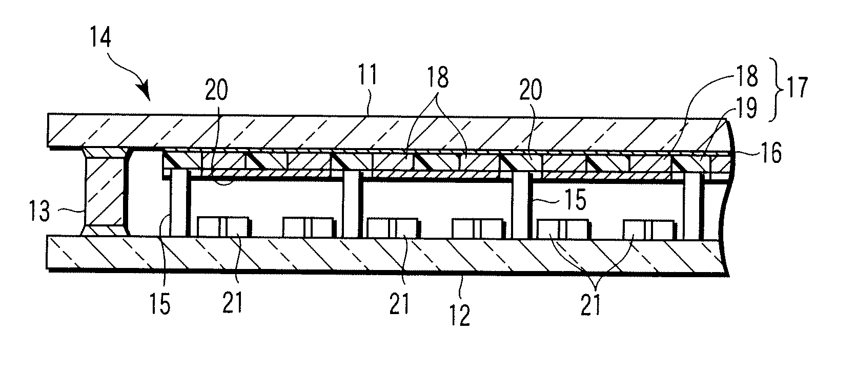
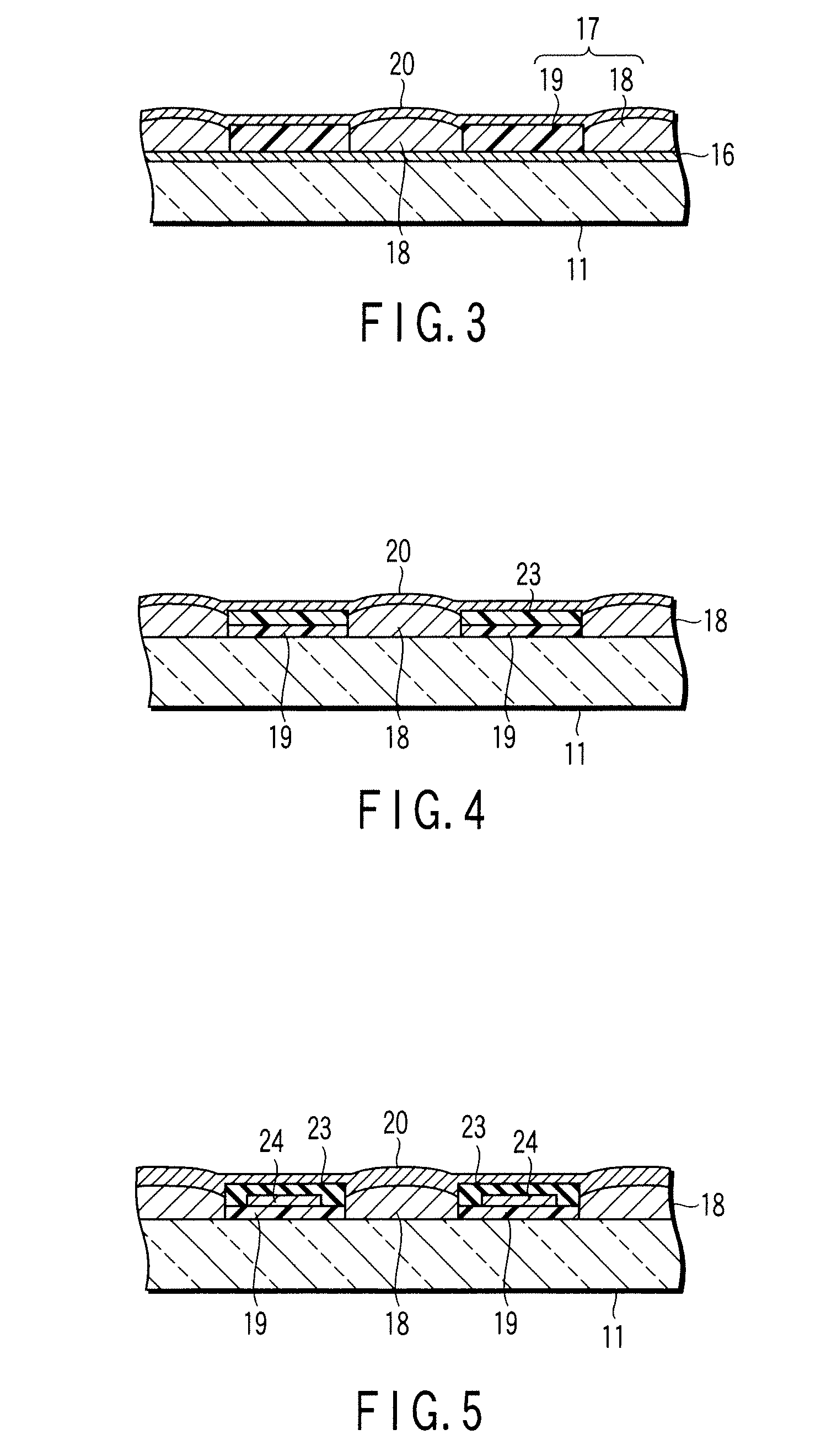
[0045]FIG. 3 shows the construction of the image display device for Example 1. The phosphor screen 17 is formed on the inner surface of the front surface substrate 11 made of glass. An ITO transparent electron conductive film 16 having a thickness of 200 nm, which performs the function of an anode power supply wiring, is formed between the front surface substrate 11 and the phosphor screen 17. Also, an anode power supply terminal (not shown), which is connected to the transparent electron conductive film 16, is connected to the inner surface of the front surface substrate 11. The phosphor screen 17 comprises phosphor layers 18 emitting light rays of red (R), green (G) and blue (B) and a light absorption layer (light shielding layer) 19 having a thickness of 10 μm, arranged in the form a matrix and including at least a part that acts as a resistance material layer. The resistance of the light shielding layer 19 that acts as the resistance material layer is set at about 1×10⁴Ω. Furthe...
example 2
[0047] As shown in FIG. 4, the image display device for Example 2 comprises a light shielding layer 19 having a thickness of 5 nm and including at least a part which acts as an anode power supply line and a resistance material layer 23 having a thickness of 10 μm and a resistance of about 1×10⁴Ω. The resistance material layer 23 is formed to cover the light shielding layer 19. Incidentally, the anode power supply terminal (not shown), which is connected to the light shielding layer 19 acting as the anode power supply wiring, is connected to the inner surface of the front surface substrate 11. The light shielding layer 19 and the metal back layer 20 are arranged to face each other with the resistance material layer 23 interposed therebetween.
[0048] The image display device for Example 2 produces effects similar to those produced by the image display device for Example 1.
example 3
[0049] As shown in FIG. 5, the image display device for Example 3 comprises an anode power supply wiring 24 having a thickness of 5 μm. The anode power supply wiring 24 is stacked on at least a part of the light shielding layer 19. Further, a resistance material layer 23 having a thickness of 10 μm and a resistance of about 1×10⁴Ω is stacked in a manner to surround the anode power supply wiring 24. Incidentally, the anode power supply terminal (not shown), which is connected to the anode power supply wiring 24, is connected to the inner surface of the front surface substrate 11. Further, the anode power supply wiring 24 and the metal back layer 20 are arranged to face each other with the resistance material layer 23 interposed therebetween.
[0050] The image display device for Example 3 produces effects similar to those produced by the image display device for Example 1.
PUM
 Abstract
Description
Claims
Application Information
 - R&D
- Intellectual Property
- Life Sciences
- Materials
- Tech Scout
- Unparalleled Data Quality
- Higher Quality Content
- 60% Fewer Hallucinations
Browse by: Latest US Patents, China's latest patents, Technical Efficacy Thesaurus, Application Domain, Technology Topic, Popular Technical Reports.
© 2025 PatSnap. All rights reserved.Legal|Privacy policy|Modern Slavery Act Transparency Statement|Sitemap|About US| Contact US: help@patsnap.com