Buried dielectric slab structure for CMOS imager

a dielectric slab and imager technology, applied in the field of semiconductor substrate wafers, can solve problems such as performance degradation and leakage or dark current in cmos imagers

Inactive Publication Date: 2007-10-25
APTINA IMAGING CORP
View PDF4 Cites 31 Cited by
  • Summary
  • Abstract
  • Description
  • Claims
  • Application Information

AI Technical Summary

Problems solved by technology

Not using such a starting substrate may cause crystal lattice defects which cause leakage or dark current in CMOS imagers.
It would be useful to create buried dielectric structures below the imager to minimize such crystal defects, but doing so typically causes performance degradation.

Method used


Image

  • Buried dielectric slab structure for CMOS imager
  • Buried dielectric slab structure for CMOS imager
  • Buried dielectric slab structure for CMOS imager

Examples


Embodiment Construction

[0018] In the following detailed description, reference is made to various specific exemplary embodiments in which the invention may be practiced. These embodiments are described with sufficient detail to enable those skilled in the art to practice the invention, and it is to be understood that other embodiments may be employed, and that structural, logical, and electrical changes may be made.

[0019] The term “substrate” used in the following description may include any semiconductor-based structure that has a semiconductor surface. For the purposes of simplification, a substrate will be described herein as a silicon substrate; however, other semiconductor substrates may also be used.

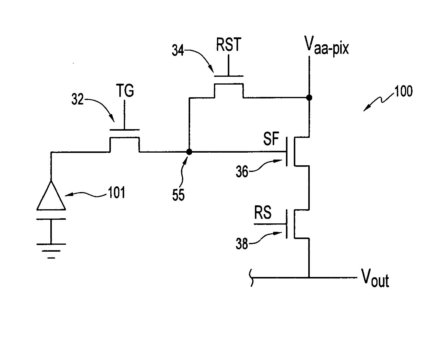
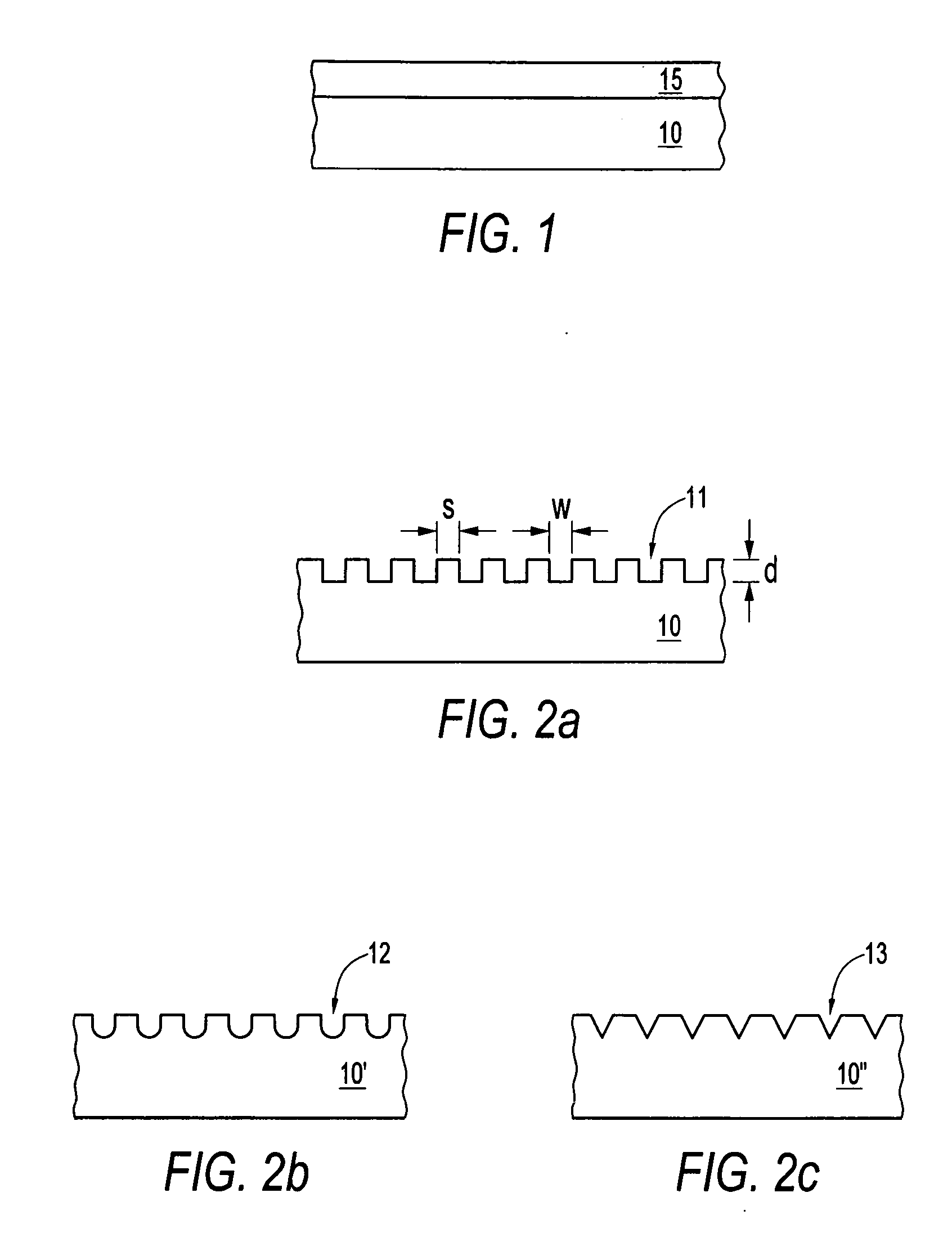
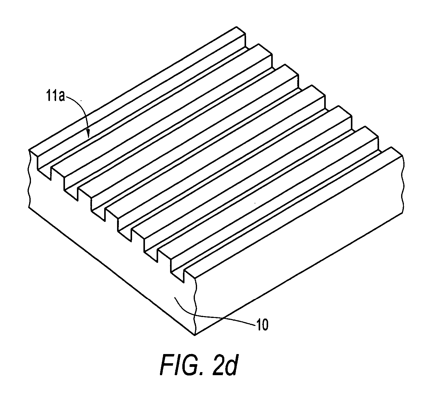
[0020] The invention discloses a substrate, system and method for creating buried dielectric structures for improving imager performance without the drawbacks of crystal defects and imager performance degradation, and at relatively low cost. Referring now to the drawings, FIG. 1 illustrates a cross-sec...


PUM

PropertyMeasurementUnit
depthaaaaaaaaaa
widthaaaaaaaaaa
dielectricaaaaaaaaaa

Abstract

A substrate structure, and method of forming the structure, are provided. The structure, which may be used for a CMOS imager device, is provided with a buried dielectric structure. Recesses are formed on a semiconductor substrate, e.g., silicon, and a dielectric material is used to fill the recesses. A layer of semiconductor material, e.g., silicon, is then formed over the surface of the substrate material and dielectric-filled trenches.

Description

FIELD OF THE INVENTION [0001] The invention relates to the field of semiconductors, and particularly, semiconductor substrate wafers. BACKGROUND OF THE INVENTION [0002] Epitaxial silicon (epi-silicon) substrate wafers are widely used in solid state imager manufacturing because they provide good dark current performance. [0003]FIG. 1 illustrates a cross-section of a semiconductor substrate 10. In conventional imager fabrication, the silicon substrate 10 is a thin layer of silicon upon which an epitaxial silicon layer 15 is formed. The epitaxial silicon grown on wafers is grown over a clean, flat wafer. Imager formation is conducted on the epitaxial layer 15. Not using such a starting substrate may cause crystal lattice defects which cause leakage or dark current in CMOS imagers. These crystals are typically caused by both non-planar geometry and use of different materials. [0004] It would be useful to create buried dielectric structures below the imager to minimize such crystal defec...

Claims


Application Information

Patent Timeline
Patent Type & Authority Applications(United States)
IPC IPC(8): H01L21/8238H01L29/80H01L21/76
CPCH01L27/14609H01L27/14689H01L27/1463
Inventor LI, JIUTAOWELLS, DAVID
Owner APTINA IMAGING CORP
Why Eureka
Try Eureka