

Chip structure with half-tunneling electrical contact to have one electrical contact formed on inactive side thereof and method for producing the same
- Summary
- Abstract
- Description
- Claims
- Application Information
AI Technical Summary
Benefits of technology
Problems solved by technology
Method used
Image

Examples
first preferred embodiment
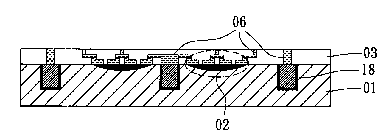
[0088]Referring now to FIG. 11a, the chip 10 of the first preferred embodiment is provided with three half-tunneling electrical contacts 18a, 18b, and 18c, each of which penetrates the processed substrate 01.
[0089]Wherein, one end of each of the half-tunneling electrical contacts 18a and 18b is exposed on the inactive side of the processed substrate 01. The other end of the half-tunneling electrical contact 18a is electrically connected to the electrical contact 05a on the active side of the chip 10 via the circuit 06 in the element layer 03 and the dielectric layer 04. Besides, the other end of the half-tunneling electrical contact 18b is electrically connected to the electrical contact 05b on the active side of the chip 10 via the semiconductor element 02 of the element layer 03 and the circuit 06 in the dielectric layer 04.
[0090]One end of the half-tunneling electrical contacts 18c is also exposed on the inactive side of the processed substrate 01, but the active side of the chip...
second preferred embodiment
[0091]Referring now to FIG. 11b, the chip 10 of the second preferred embodiment is provided with a plurality of electrical contacts 05, all of which are only exposed on the inactive side of the processed substrate 01.
third preferred embodiment
[0092]Referring now to FIG. 11c, the chip 10 of the third preferred embodiment is provided with a plurality of electrical contacts 05 which are exposed on the active side and the inactive side of the processed substrate 01.
PUM
 Abstract
Description
Claims
Application Information