Dielectric Metasurface Optical Elements

Active Publication Date: 2016-01-28
THE BOARD OF TRUSTEES OF THE LELAND STANFORD JUNIOR UNIV +1
View PDF19 Cites 89 Cited by
  • Summary
  • Abstract
  • Description
  • Claims
  • Application Information

AI Technical Summary

Benefits of technology

[0012]Significantly, embodiments of the invention use optically resonant high-index nanostructure to realize PBOEs and optical metasurfaces. These PBOE optical elements can perform a range of optical functions in a form factor that is much thinner than before. This allows easy fabrication and integration with semiconductor electronics and other planar technologies. It also allows for easy stacking of optical planar components. Possibly all optical applications where refractive optics are used may benefit from such devices, including optical imaging, sensing, light trapping, optical communication technology, beam steering, and thermal emission control. It also has applications in sensing, light trapping, optical communication technology, beam steering, and thermal emission control. Industries that may benefit include communications companies, optics companies, bio(sensing) companies, defense related companies and display companies.
[0013]Building upon recent advances in the realization of high-index dielectric antennas as well as upon Pancharatnam-Berry phase optical elements (PBOEs), the present invention provides easy-to-fabricate and highly-efficient transm

Problems solved by technology

These traditional optical components are bulky and suffer from various well-known effects such as chromatic aberration.
These designs, however, suffer from Ohmic losses in the metal.
These metals, however, only work well in the infrared and microwave spectral regions.
At and near visible wavelengths, they suffer from high losses arising in part from interband transitions.
Also, due to the limited scattering cross sections of the antennas, these devices have efficiencies only in reflection mode.
Consequently, they are unsuitable for use in transmission mode.
In addition, noble metals are not compatible

Method used


Image

  • Dielectric Metasurface Optical Elements
  • Dielectric Metasurface Optical Elements
  • Dielectric Metasurface Optical Elements

Examples


Example

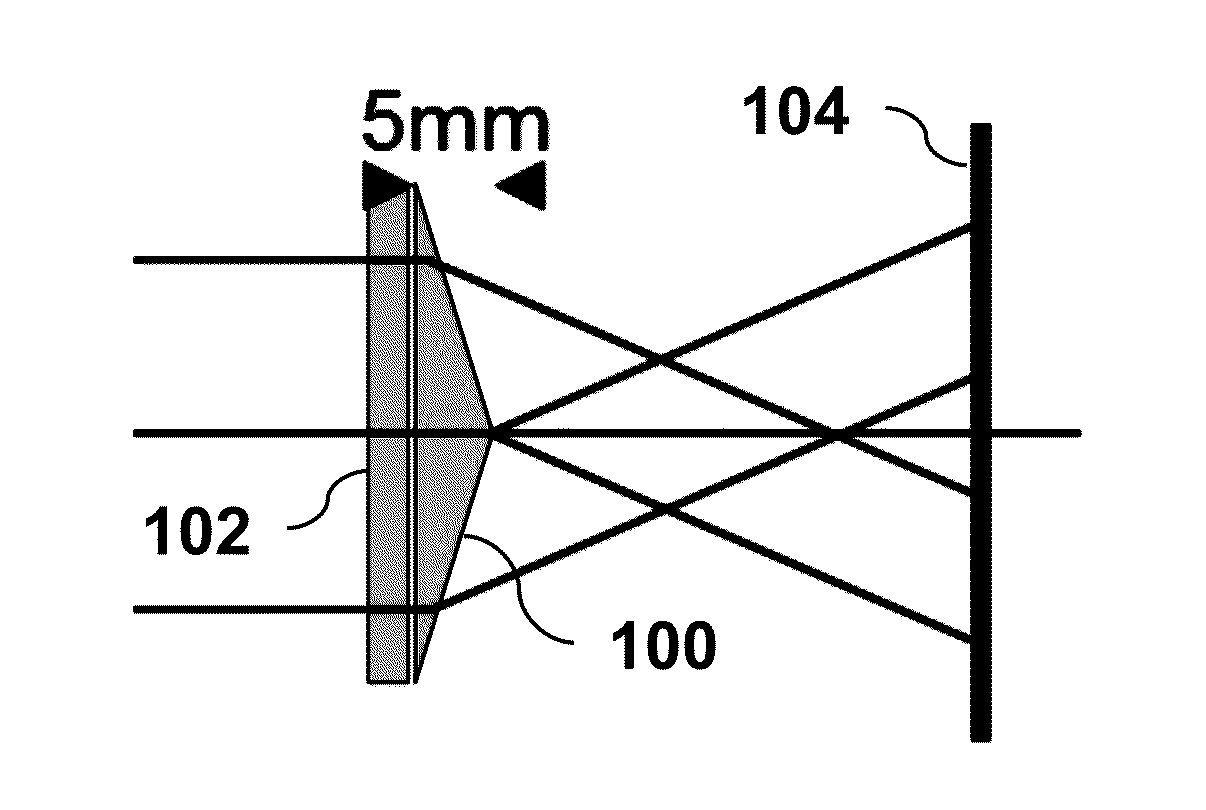
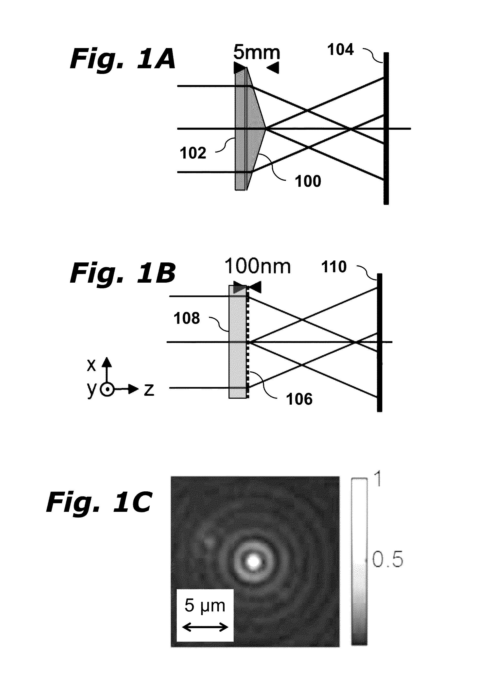
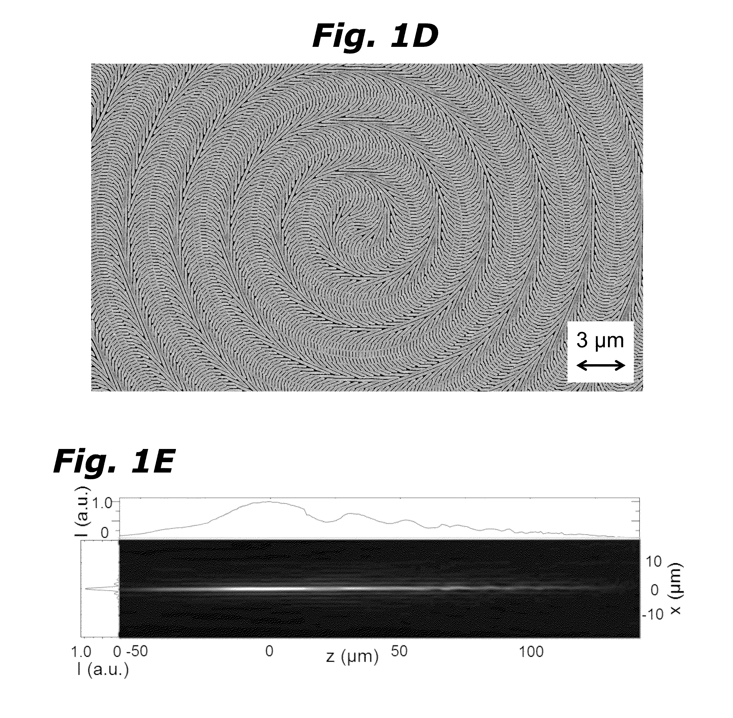
[0044]Embodiments of the present invention provide devices employing gradient metasurfaces, which are essentially 2-dimensional optical elements capable of manipulating light by imparting local, space-variant phase-changes on an incident electromagnetic wave. These surfaces have previously been constructed from nanometallic optical antennas and high diffraction efficiencies have been limited to operation in reflection mode. The present invention provides a realization of dielectric gradient metasurface optical elements (DGMOEs) capable of achieving high efficiencies in transmission mode at visible wavelengths. Embodiments include ultrathin gratings, lenses, and axicons that may be realized by judiciously patterning a 100-nm-thin Si layer into a dense arrangement of Si nanobeam-antennas. By fabricating these gradient metasurfaces with silicon and other semiconductor materials, they can be integrated with electronic, electrooptic, and electromechanical devices using mature semiconduct...


PUM


Abstract

A dielectric gradient metasurface optical device provides optical wavefront shaping using an ultrathin (less than 100 nm thick) layer of nanoscale geometric Pancharatnam-Berry phase optical elements deposited on a substrate layer. The optical elements are nanobeams composed of high refractive index dielectric material. The nanobeams have uniform size and shape and are arranged with less than 200 nm separations and spatially varying orientations in the plane of the device such that the optical device has a spatially varying optical phase response capable of optical wavefront shaping. The high refractive index dielectric material may be materials compatible with semiconductor electronic fabrication, including silicon, polysilicon, germanium, gallium arsenide, titanium dioxide, or iron oxide.

Description

BACKGROUND OF THE INVENTION[0001]Traditional optical components such as glass lenses shape the wavefront of an incident light beam using variations in thickness to create different optical path lengths. The thickness of such components is much larger than the wavelength. These traditional optical components are bulky and suffer from various well-known effects such as chromatic aberration. Advances in technology in recent decades has led to a new class of flat, ultrathin optical components based on metasurfaces. A metasurface is a quasi-two-dimensional structure composed of resonant optical antenna elements arranged to form subwavelength-patterned structures that interact strongly with light. Metasurfaces can be used to manipulate the propagation of light by spatially varying geometric parameters of the structures (e.g., antenna shape, size, orientation) to provide a spatially varying optical response that molds optical wavefronts as desired. The optical antenna elements alter light ...

Claims


Application Information

Patent Timeline
IPC IPC(8): G02B5/30G02B5/00G02B5/18
CPCG02B5/3083G02B5/1833G02B5/001G02B1/002B82Y20/00
Inventor BRONGERSMA, MARK L.LIN, DIANMINFAN, PENGYUHASMAN, EREZ
Owner THE BOARD OF TRUSTEES OF THE LELAND STANFORD JUNIOR UNIV
Why Eureka
Try Eureka