Boosting methods for NAND flash memory

a boosting method and flash memory technology, applied in static storage, digital storage, instruments, etc., can solve the problems of low level caused by such a high boosting voltage (boosting voltage disturbance) and achieve the effect of reducing programming voltage, high boosting voltage, and high boosting voltag

Inactive Publication Date: 2007-11-08
SANDISK TECH LLC
View PDF42 Cites 34 Cited by
  • Summary
  • Abstract
  • Description
  • Claims
  • Application Information

AI Technical Summary

Benefits of technology

[0027] A higher boosting voltage applied to a word line adjacent to the selected word line tends to couple to a selected floating gate (a floating gate under the selected word line). Thus, the higher boosting voltage works with the programming voltage to cause charging of the floating gate. However, by only applying higher boosting voltage to a limited number of word lines, problems caused by such higher boosting voltage (boosting voltage disturb) are kept at a low level. By applying a series of descending voltages to word lines near a selected word line, an appropriate balance is maintained between the advantages of higher boosting voltage (coupling higher voltage to selected floating gates and to the channel), which increase closer to the selected word line, and the disadvantages of higher boosting voltage (boosting voltage disturb), which are generally not dependent on distance from the selected word line. Using a high boosting voltage for word lines adjacent to the selected word line assists in causing charge to flow to floating gates and may allow a reduced programming voltage to be used, thus reducing Vpgm-disturbs.

Problems solved by technology

However, by only applying higher boosting voltage to a limited number of word lines, problems caused by such higher boosting voltage (boosting voltage disturb) are kept at a low level.

Method used


Image

  • Boosting methods for NAND flash memory
  • Boosting methods for NAND flash memory
  • Boosting methods for NAND flash memory

Examples


Embodiment Construction

[0047]FIG. 5 shows a cross section of a portion of a NAND string in a flash memory array undergoing programming according to an embodiment of the present invention. FIG. 5 shows capacitors representing capacitive coupling between some of the elements of the NAND string. Not all couplings between elements are shown. For example, word lines are strongly coupled to directly underlying floating gates allowing floating gates to be programmed. Also, both floating gates and word lines are coupled to a portion of the underlying substrate. The particular couplings shown are chosen to illustrate some of the advantages of this embodiment over prior art programming schemes. Also, the couplings shown are becoming more significant as lateral dimensions of NAND arrays are scaled down in size more rapidly than vertical dimensions are scaled.

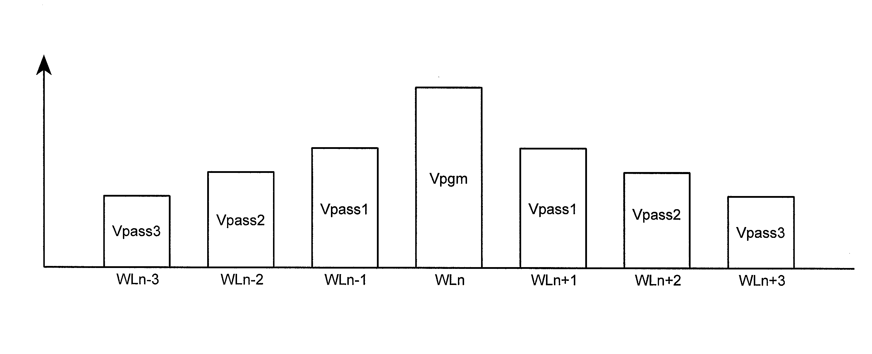
[0048]FIG. 6 shows voltages applied to word lines WLn−3 to WLn+3 of FIG. 5 according to one embodiment of the present invention. WLn is the selected word line ...


PUM


Abstract

A floating gate memory array includes row control circuits that provide a programming voltage to a selected word line and provide a stair-like pattern of boosting voltages to unselected word lines. Boosting voltages descend with increased distance from the selected word line. Boosting voltages are increased in small increments up to their final values.

Description

CROSS-REFERENCE TO RELATED APPLICATIONS [0001] This application is related to U.S. patent application Ser. No. ______, entitled, “NAND Flash Memory with Boosting,” filed on the same day as the present application; which application is incorporated herein as if fully set forth in its entirety.BACKGROUND OF THE INVENTION [0002] This invention relates generally to non-volatile semiconductor memories of the flash EEPROM (Electrically Erasable and Programmable Read Only Memory) type, particularly to structures and methods of operating NAND types of memory cell arrays. All patents, patent applications and other material cited in the present application are hereby incorporated by reference in their entirety. [0003] There are many commercially successful non-volatile memory products being used today, particularly in the form of small form factor cards, which use an array of flash EEPROM cells. [0004] An example memory system is illustrated by the block diagram of FIG. 1. A memory cell array...

Claims


Application Information

Patent Timeline
Patent Type & Authority Applications(United States)
IPC IPC(8): G11C16/04G11C11/34
CPCG11C16/3427G11C16/3418
Inventor HIGASHITANI, MASAAKI
Owner SANDISK TECH LLC
Why Eureka
Try Eureka