Coupling electromagnetic wave through microcircuit

a micro-circuit and electromagnetic wave technology, applied in the field of coupling signals, can solve the problems of loss of synchronization, micro-circuit cannot function correctly, and the device speed is generally limited,

Active Publication Date: 2007-11-08
ADVANCED PLASMONICS
View PDF99 Cites 37 Cited by
  • Summary
  • Abstract
  • Description
  • Claims
  • Application Information

AI Technical Summary

Problems solved by technology

This improvement in device speed is generally limited by the conductors between the devices.
As the clock speeds increase, the conductor delays can result in a loss in synchronization such that the microcircuit cannot function correctly.
As the requirements for speed further increase, any improvement in reducing delays by changing the conductor and dielectric layer materials are limited.
The costs for changing the geometry of the conductor can include more processing steps and push the limits of the statistical capability of the process.

Method used


Image

  • Coupling electromagnetic wave through microcircuit
  • Coupling electromagnetic wave through microcircuit
  • Coupling electromagnetic wave through microcircuit

Examples


Embodiment Construction

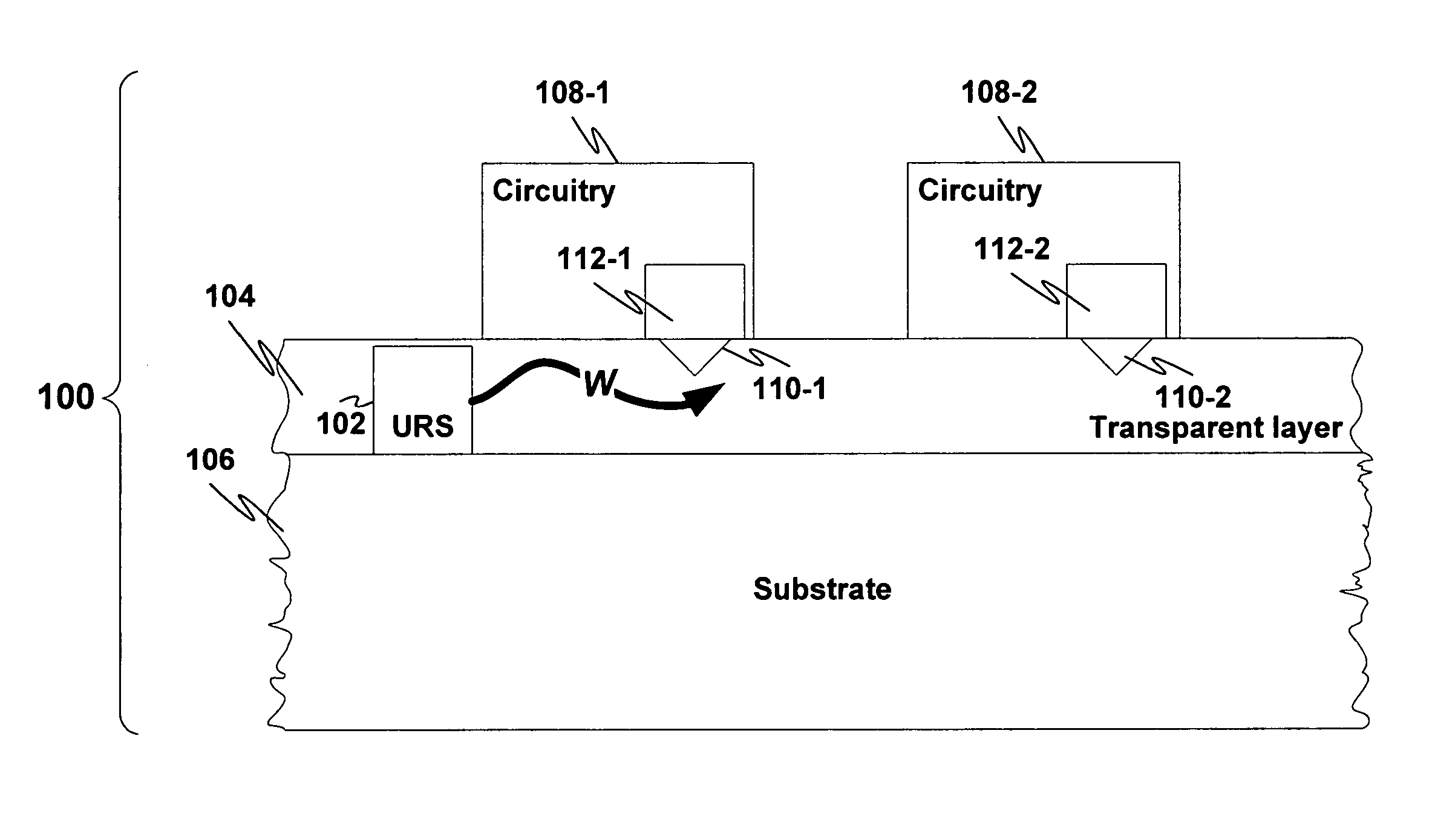
[0021]FIG. 1 is a side view of a device 100 in which an ultra-small resonant structure 102 is formed within a non-conductive waveguide layer 104 on a substrate 106.

[0022] In general, the ultra-small resonant structure is one which emits electromagnetic radiation (EMR) when exposed to a beam of charged particles. The structure 102 may be, e.g., one or more of the resonant structures described in one or more of the related applications, each of which is described in greater detail above: U.S. application Ser. Nos. 11 / 243,476; 11 / 243,477; 11 / 238,991; 11 / 302,471; 11 / 325,432; 11 / 325,448; 11 / 325,571; and 11 / 325,534. In particular, the structure 102 may be one which emits light at a particular wavelength, e.g., visible light. Thus, the ultra-small resonant structure 102 emits an EMR wave (denoted W) in the waveguide layer 104. The wave W may be modulated or otherwise manipulated to carry a data signal such as, e.g., a clock signal.

[0023] The waveguide layer 104 is preferably transparent ...


PUM


Abstract

A device includes a waveguide layer formed on a substrate. An ultra-small resonant structure emits electromagnetic radiation (EMR) in the waveguide layer. One or more circuits are formed on the waveguide layer and each operatively connected thereto to receive the EMR emitted by the ultra-small resonant structure. The waveguide layer may be transparent at wavelengths corresponding to wavelengths of the EMR emitted by the ultra-small resonant structure. The EMR may be visible light and may encode a data signal such as a clock signal.

Description

RELATED APPLICATIONS [0001] The present invention is related to the following co-pending U.S. Patent applications, each which is commonly owned with the present application at the time of filing, and the entire contents of each of which are incorporated herein by reference: [0002] 1. application Ser. No. 10 / 917,571, filed on Aug. 13, 2004, entitled “Patterning Thin Metal Film by Dry Reactive Ion Etching”; [0003] 2. application Ser. No. 11 / 203,407, filed Aug. 15, 2005, entitled “Method of Patterning Ultra-Small Structures,”[0004] 3. application Ser. No. 11 / 243,476, filed Oct. 5, 2005, entitled, “Structure and Methods for Coupling Energy from an Electromagnetic Wave”; [0005] 4. application Ser. No. 11 / 243,477, filed Oct. 5, 2005, entitled, “Electron Beam Induced Resonance”; [0006] 5. application Ser. No. 11 / 238,991, filed Sep. 30, 2005, entitled, “Light Emitting Free-Electron Micro Resonant Structure”; [0007] 6. application Ser. No. 11 / 302,471, filed Dec. 14, 2005, entitled, “Coupled ...

Claims


Application Information

Patent Timeline
Patent Type & Authority Applications(United States)
IPC IPC(8): G02B6/10
CPCH01J25/02G02B6/43
Inventor GORRELL, JONATHANDAVIDSON, MARKMAINES, MICHAEL E.
Owner ADVANCED PLASMONICS
Why Eureka
Try Eureka