Correcting apparatus for wafer transport equipment and correcting method for wafer transport equipment

a technology of wafer transport equipment and correcting apparatus, which is applied in the direction of instruments, computing, electric digital data processing, etc., can solve the problems of difficulty for operators to recognize the offset in the height of even one mechanical arm, inconvenient operation, and inability to accurately correct the wafer transport equipment. , to achieve the effect of avoiding damage to the wafer and accurately correcting the wafer transport equipmen

Inactive Publication Date: 2007-11-08
POWERCHIP SEMICON CORP
View PDF5 Cites 11 Cited by
  • Summary
  • Abstract
  • Description
  • Claims
  • Application Information

AI Technical Summary

Benefits of technology

[0008]Accordingly, an objective of the present invention is to provide a correcting apparatus for wafer transport equipment, which can accurately correct the wafer transport equipment so as to avoid damage to a wafer when picking up and placing the wafer.

Problems solved by technology

The above correcting method often results in an incorrect location of the mechanical arm due to the factors such as different viewing angles of the operators and subjective judgment from different operators.
Thus, the mechanical arm may scrape or crack the wafer when picking up or placing the wafer.
In addition, in a plurality of mechanical arms 111˜115, it is difficult for the operator to recognize the offset in the height of even one mechanical arm (for example, the mechanical arm 113).
Therefore, the method for correcting the location of the mechanical arm by eyes in the conventional art cannot accurately and efficiently adjust the location of the mechanical arm, especially the locations of a plurality of mechanical arms.

Method used


Image

  • Correcting apparatus for wafer transport equipment and correcting method for wafer transport equipment
  • Correcting apparatus for wafer transport equipment and correcting method for wafer transport equipment
  • Correcting apparatus for wafer transport equipment and correcting method for wafer transport equipment

Examples


Embodiment Construction

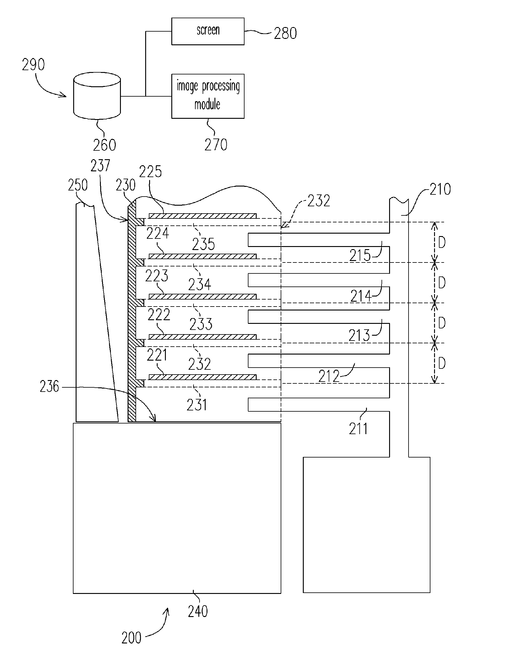
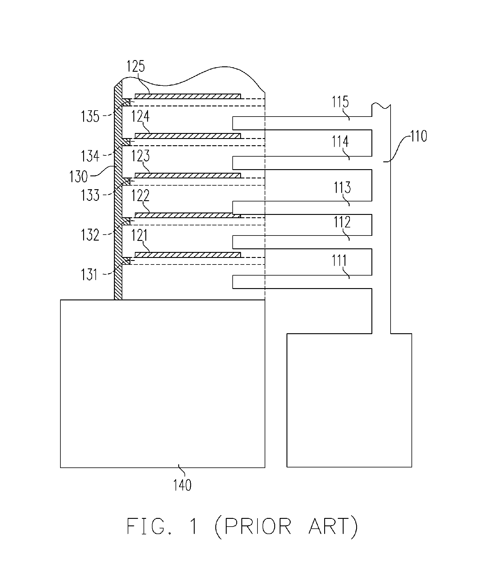
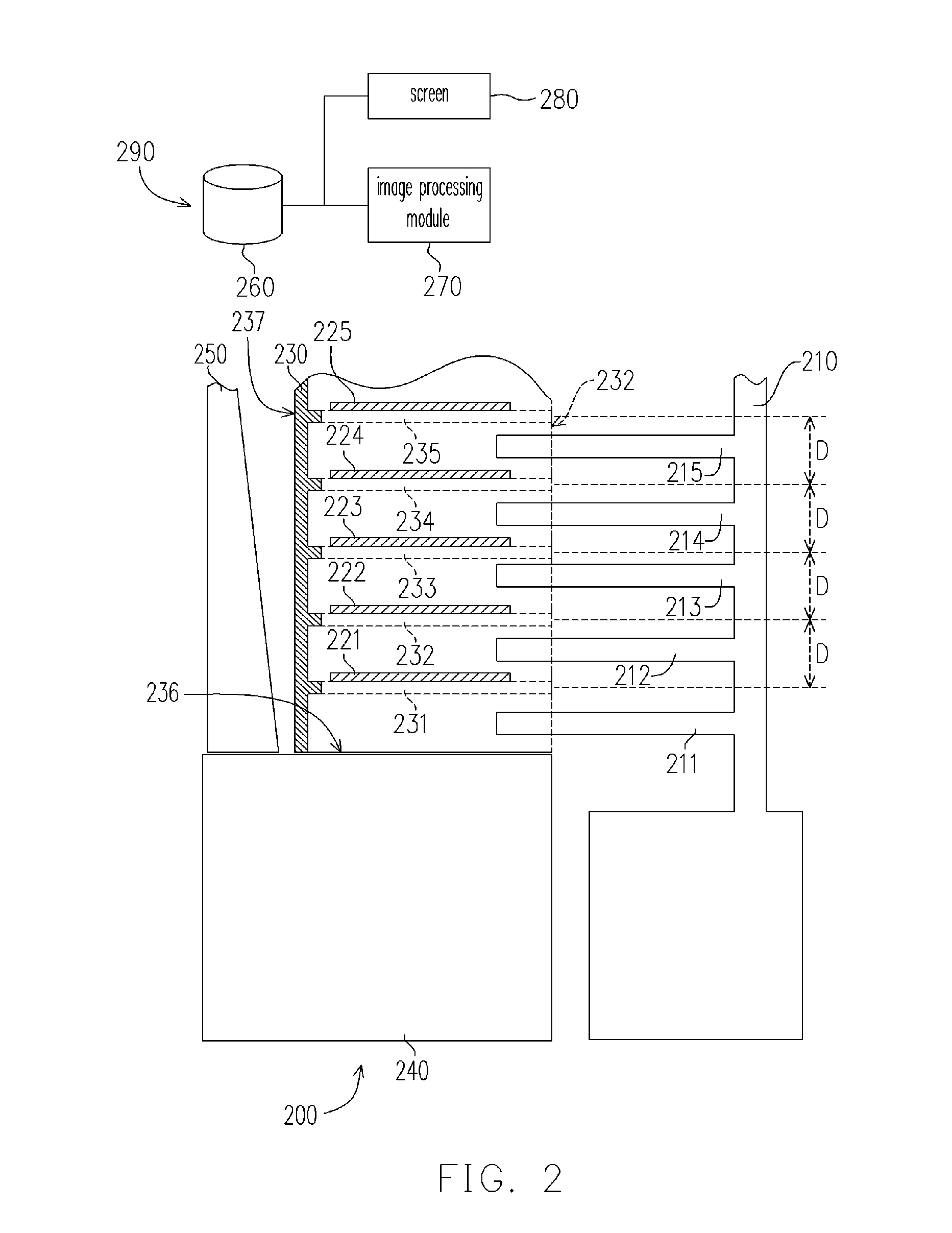
[0022]In the semiconductor process, the conveyer is often used to move wafers to or from the wafer carrying device or various different tables, so as to perform different processes. As in the conventional art the mechanical arm is corrected by human eyes observing whether the location thereof is correct or not, it is likely to cause misjudgment. Therefore, the present invention provides a correcting apparatus for wafer transport equipment and a correcting method for wafer transport equipment to accurately correct the mechanical arm, thereby avoiding damage to the wafer when being transported. Here, the embodiments are used to illustrate the present invention instead of limiting the present invention. Some modifications can be made to the embodiments below by those skilled in the art according to the spirit of the present invention, which still belong to the scope of the present invention.

[0023]FIG. 2 is a schematic view of a wafer transport equipment and a correcting apparatus there...


PUM


Abstract

A correcting apparatus for wafer transport equipment is provided. The correcting apparatus includes a reflective component, an image capture module, an image processing module and a screen. The reflective component is disposed near a wafer carrying device to reflect an image of the wafer carrying device to the image capture module. The image capture module is disposed in the optical path of the reflected light of the reflective component to capture the image in the wafer carrying device. The image capture module is coupled to the image processing module. When a conveyer stretches into the wafer carrying device, the image processing module analyzes the image captured by the image capture module to determine whether the location of the conveyer is correct or not. The location of the conveyer is accurately and immediately adjusted according to the result of the analysis.

Description

CROSS-REFERENCE TO RELATED APPLICATION[0001]This application claims the priority benefit of Taiwan application serial no. 95116006, filed on May 5, 2006. All disclosure of the Taiwan application is incorporated herein by reference.BACKGROUND OF THE INVENTION[0002]1. Field of Invention[0003]The present invention relates to a correcting apparatus for wafer transport equipment. More particularly, the present invention relates to a correcting apparatus for wafer transport equipment and a correcting method for wafer transport equipment via a computer.[0004]2. Description of Related Art[0005]In the workshop for manufacturing semiconductor wafers, a precision mechanical arm is usually used to transport wafers. Before using the mechanical arm to transport wafers, it is necessary to correct the location of the mechanical arm to avoid damage to the wafers due to the improper location of the mechanical arm. For various mechanical arms provided at present, the locations of most mechanical arms ...

Claims


Application Information

Patent Timeline
Patent Type & Authority Applications(United States)
IPC IPC(8): G06F19/00
CPCH01L21/67265
Inventor WU, CHAN-TSUNLIN, PETER
Owner POWERCHIP SEMICON CORP
Why Eureka
Try Eureka