Semiconductor memory device

a semiconductor memory and memory device technology, applied in the field of semiconductor memory devices, can solve the problems of increasing the workload of the host device, increasing the error rate with an increase in the number of data rewrite operations, and electrically rewritable and non-volatile semiconductor memory devices,

Inactive Publication Date: 2007-11-15
KK TOSHIBA
View PDF37 Cites 124 Cited by
  • Summary
  • Abstract
  • Description
  • Claims
  • Application Information

AI Technical Summary

Problems solved by technology

Electrically rewritable and non-volatile semiconductor memory devices, i.e., flash memories, increase in error rate with an increase in number of data rewrite operations.
In particular, the further enhancement of the storage capacity increase and miniaturization results in the error rate increase.
In this case, however, the host device increases in its workload when the error rate is increased.

Method used


Image

  • Semiconductor memory device
  • Semiconductor memory device
  • Semiconductor memory device

Examples


Embodiment Construction

[0062]Previously to the detailed explanation of the embodiments, background and outline thereof will be explained below.

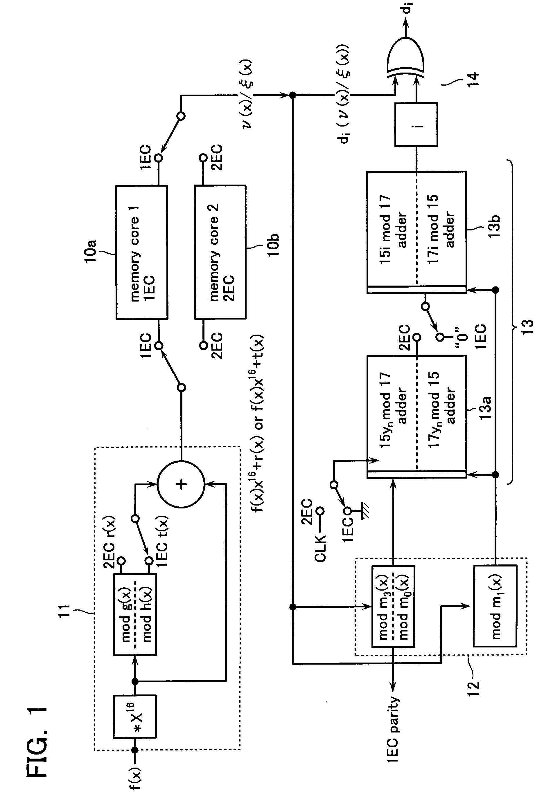
[0063]Miniaturization of the cell array and capacity-increase being enhanced in a semiconductor memory, it becomes necessary to use an error detection and correction system (ECC system) for securing the data reliability. However, to mount an ECC system, it is in need of preparing a check bit area in addition to a normal data storage area. Particularly, to achieve a high-powered ECC system, it is required to prepare a large check bit area.

[0064]That is, to secure the data reliability, it is necessary to take a large check bit area, while increasing of the check bit area leads to reduction of the normal data area, thereby resulting in that it takes a long time for error correcting. Therefore, the data reliability is inconsistent with the data area efficiency and error-correcting speed.

[0065]For example, in a BCH code system, which is 2-bit error correctable, i.e., 2E...


PUM


Abstract

A semiconductor memory device including an error detection and correction system, wherein the error detection and correction system has a first operation mode for correcting one number-bit (for example 2) errors and a second operation mode for correcting another number-bit (for example 1) error(s), which are exchangeable to be set with a main portion of the system used in common.

Description

CROSS-REFERENCE TO RELATED APPLICATION[0001]This application is based on and claims the benefit of priority from the prior Japanese Patent Application No. 2006-135025, filed on May 15, 2006, the entire contents of which are incorporated herein by reference.BACKGROUND OF THE INVENTION[0002]1. Field of the Invention[0003]This invention relates to a semiconductor memory device, and more specifically, to an error detection and correction system integrally formed in the device.[0004]2. Description of the Related Art[0005]Electrically rewritable and non-volatile semiconductor memory devices, i.e., flash memories, increase in error rate with an increase in number of data rewrite operations. In particular, the further enhancement of the storage capacity increase and miniaturization results in the error rate increase. In view of this, an attempt is made to mount a built-in error correcting code (ECC) circuit on flash memory chips or memory controllers of these memories. An exemplary device u...

Claims


Application Information

Patent Timeline
Patent Type & Authority Applications(United States)
IPC IPC(8): G06F11/00H03M13/00
CPCG06F11/1068H03M13/1575H03M13/152
Inventor TODA, HARUKIEDAHIRO, TOSHIAKI
Owner KK TOSHIBA
Why Eureka
Try Eureka