

Drive voltage supply circuit
- Summary
- Abstract
- Description
- Claims
- Application Information
AI Technical Summary
Benefits of technology
Problems solved by technology
Method used
Image

Examples
embodiment 1
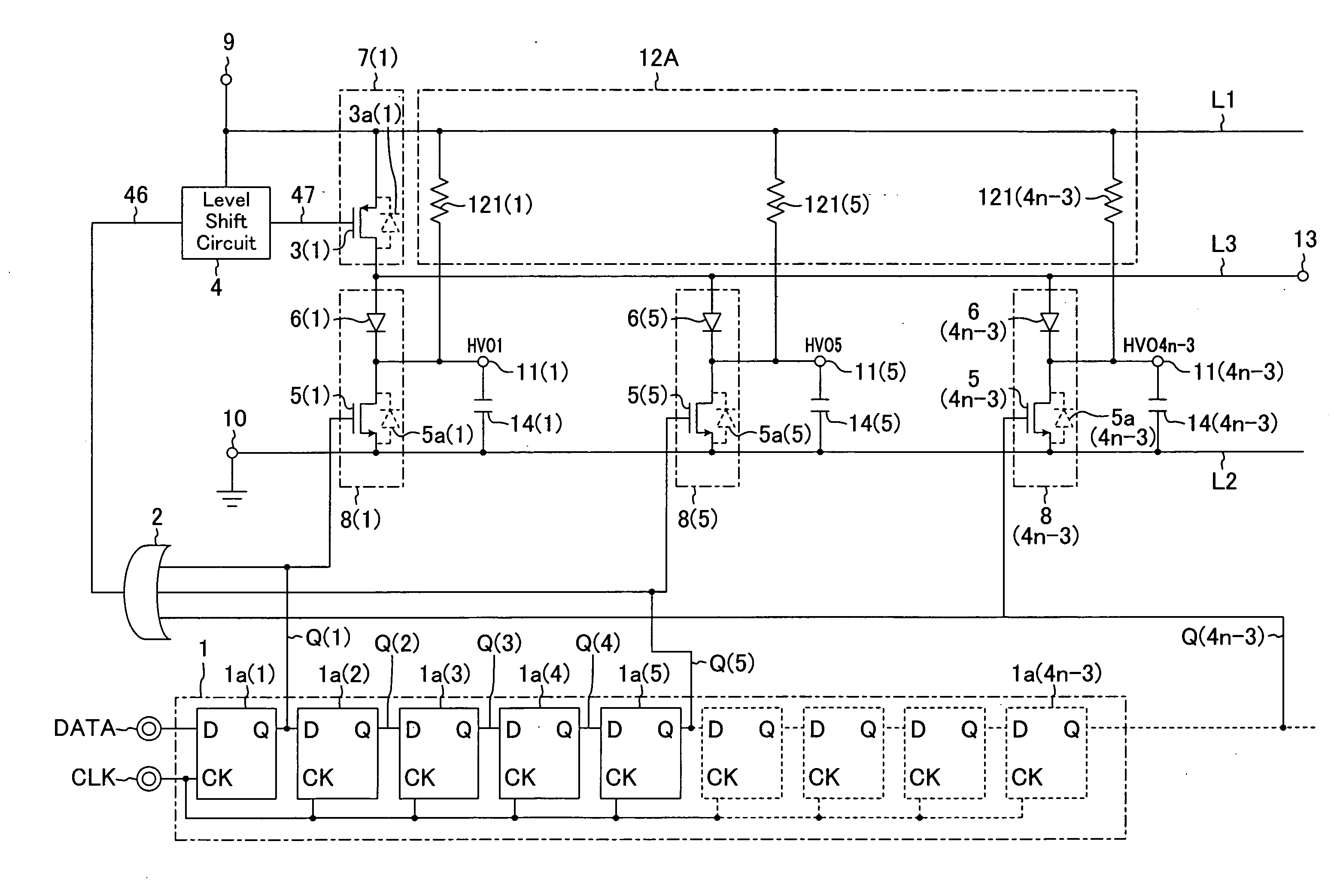
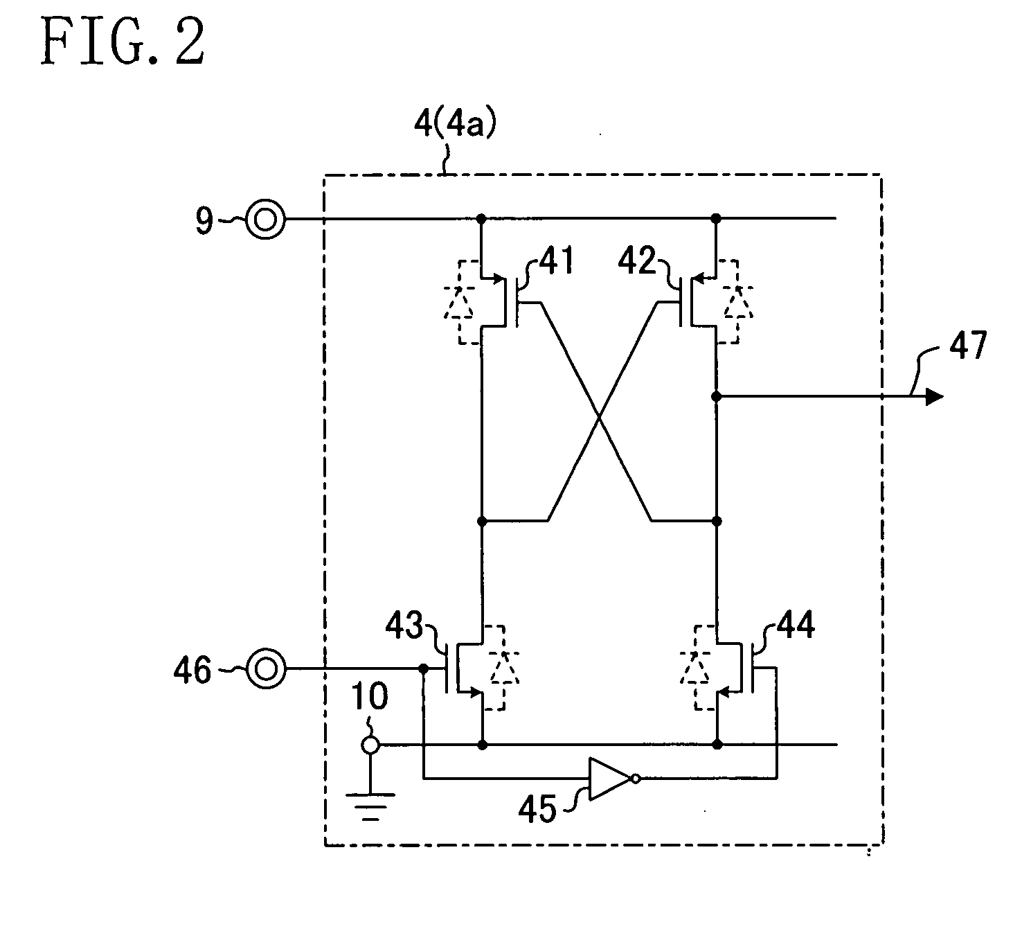
[0038]A drive voltage supply circuit according to the first embodiment of the present invention is used in a multi-channel semiconductor integrated circuit and features a structure in which resistors are provided between a power source terminal and output terminals. The structure allows a current to flow between the power source terminal and each of capacitive loads connected to the output terminals during a period other than the period in which the potentials at the output terminals are on the H level. As a result, it is possible to suppress an oscillation in the potential at each of the output terminals due to a disturbance when each of a high-side transistor and low-side transistors is OFF and a HIZ state occurs.
[0039]A specific description will be given herein below to the drive voltage supply circuit according to the first embodiment.
[0040]FIG. 1 shows a structure of the drive voltage supply circuit according to the first embodiment in a multi-channel semiconductor integrated c...
embodiment 2
[0073]A drive voltage supply circuit according to the second embodiment of the present invention is characterized in that a constant current source is provided between the power source terminal and the output terminals. As a result, when the potential at any of the capacitive loads connected to the output terminals is lower than the potential at the power source, a constant current is allowed to flow in the capacitive load. The arrangement suppresses an oscillation in the potential at each of the output terminals due to a disturbance when each of the high-side transistor and low-side transistors is OFF and the HIZ state occurs.
[0074]A specific description will be given herein below to the drive voltage supply circuit according to the second embodiment.
[0075]FIG. 5 shows a structure of the drive voltage supply circuit according to the second embodiment in a multi-channel semiconductor integrated circuit. For easy description of the operation, the connection of each of the capacitive ...
embodiment 3
[0091]A drive voltage supply circuit according to the third embodiment of the present invention is characterized in that a constant current source controlled by switches is provided between the power source terminal and the output terminals. As a result, when the potential at any of the capacitive loads connected to the output terminals is lower than the potential at the power source and the potential at the output terminal is on the L level, a constant current is allowed to flow in the capacitive load. The arrangement suppresses an oscillation in the potential at each of the output terminals due to a disturbance when each of the high-side transistor and the low-side transistors is OFF and the HIZ state occurs, while efficiently supplying the current to the capacitive load during the period in which the oscillation in output potential is not desired.
[0092]A specific description will be given herein below to the drive voltage supply circuit according to the third embodiment.
[0093]FIG...
PUM
 Abstract
Description
Claims
Application Information