

Semiconductor device
a technology of semiconductors and devices, applied in the direction of insulated conductors, cables, instruments, etc., can solve the problems of reducing yield, and affecting the performance of the devi
- Summary
- Abstract
- Description
- Claims
- Application Information
AI Technical Summary
Benefits of technology
Problems solved by technology
Method used
Image

Examples
first embodiment
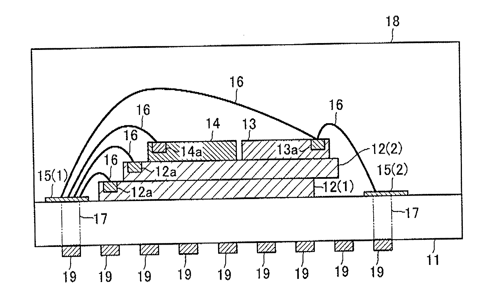
[0031]FIG. 1 is referenced to describe a semiconductor device according to a first embodiment of the present invention. FIG. 1 is a brief diagram of the semiconductor device according to the first embodiment.
[0032] As shown in FIG. 1, the semiconductor device according to the first embodiment of the present invention comprises a package board 11, semiconductor chips 12(1), 12(2) stacked on the package board 11, a memory controller 13 arranged on the semiconductor chip 12(2), and a power supply chip 14 having a capacitor function inside. The semiconductor chips 12(1), 12(2) may include, but not particularly limited to, storage devices such as NAND-type flash memories. The semiconductor chips 12(1), 12(2), the memory controller 13 and the power supply chip 14 have respective electrically connectable bonding pads 12a, 12a, 13a, 14a formed thereon. To prevent the bonding pads 12a, 13a from overlapping and remaining hidden (in other words, to enable bonding), the two semiconductor chips...
second embodiment
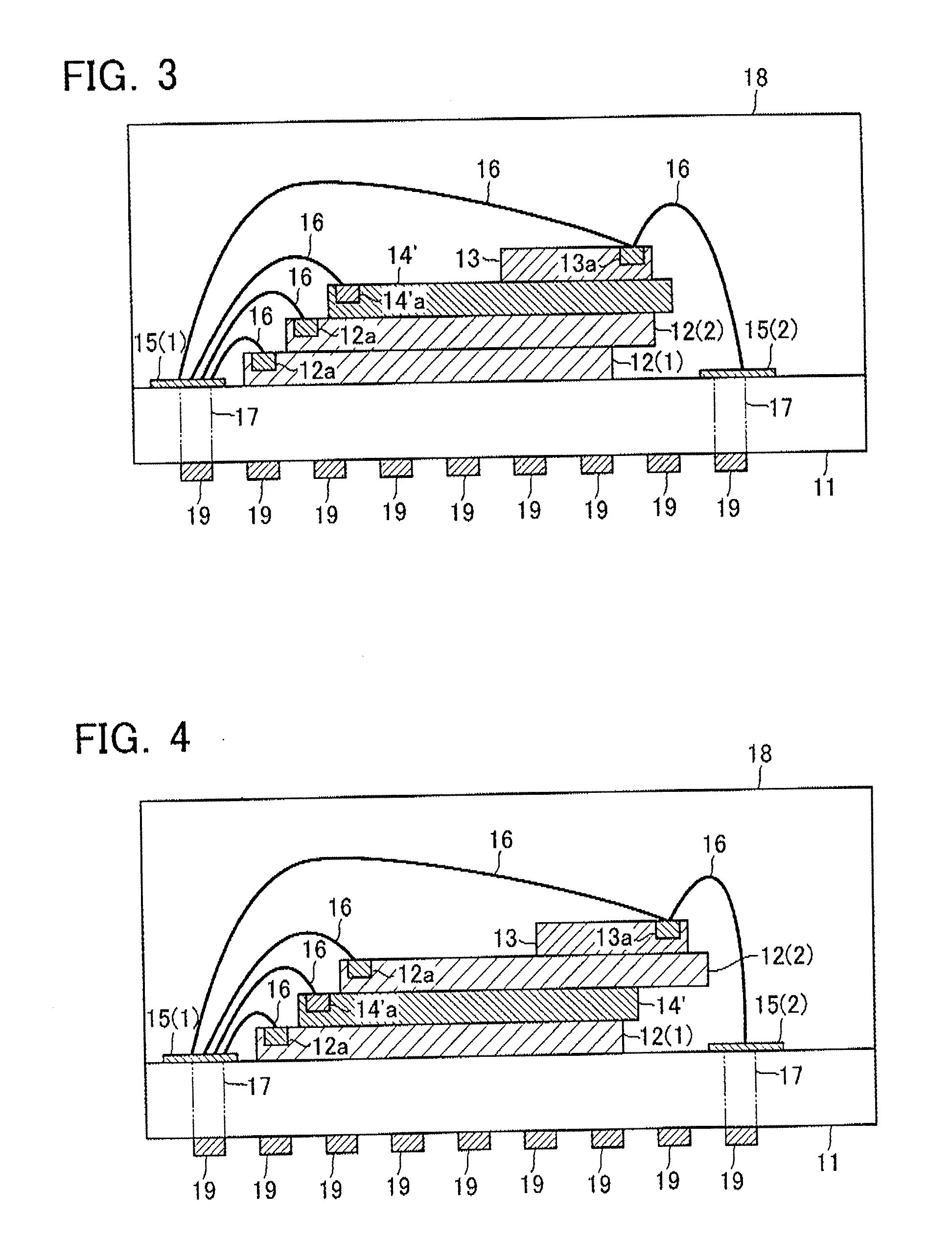
[0042]FIG. 3 is referenced next to describe a configuration of a semiconductor device according to a second embodiment of the present invention. FIG. 3 is a side view showing the configuration of the semiconductor device according to the second embodiment of the present invention. The same components as those in the first embodiment are denoted with the same reference numerals and omitted from the following description.
[0043] As shown in FIG. 3, different from the first embodiment, in the semiconductor device according to the second embodiment, a power supply chip 14′ is formed having as large a size as extending over the entire surface of the semiconductor chip 12(2). In addition, the memory chip 13 is stacked on the power supply chip 14′. To prevent bonding pads 12a, 12a, 14′ a from overlapping and remaining hidden (in other words, to enable bonding), the two semiconductor chips 12(1), 12(2) and the power supply chip 14′ are stacked as deviated so that one ends thereof are arrang...
third embodiment
[0045]FIG. 4 is referenced next to describe a configuration of a semiconductor device according to a third embodiment of the present invention. FIG. 4 is a side view showing the configuration of the semiconductor device according to the third embodiment of the present invention. The same components as those in the second embodiment are denoted with the same reference numerals and omitted from the following description.
[0046] As shown in FIG. 4, in the semiconductor device according to the third embodiment, to prevent bonding pads 12a, 12a, 13a, 14′a from overlapping and remaining hidden (in other words, to enable bonding), the semiconductor chip 12(1), the power supply chip 14′, the semiconductor chip 12(2) and the memory chip 13 are stacked as deviated so that one ends thereof are arranged in a stepwise form on the package board 11 in this order, which is different from that in the second embodiment. In other word, the power supply chip 14′ is interposed between the semiconductor ...
PUM
 Abstract
Description
Claims
Application Information