
Image display device

a display device and image technology, applied in static indicating devices, instruments, electroluminescent light sources, etc., can solve the problems of difficult to realize a large display device having a high definition, and achieve the effect of reducing the number of gate lines, reducing the crossover between wirings, and improving the yield of the panel

Inactive Publication Date: 2007-11-29
SONY CORP
View PDF18 Cites 56 Cited by
  • Summary
  • Abstract
  • Description
  • Claims
  • Application Information

AI Technical Summary

Benefits of technology

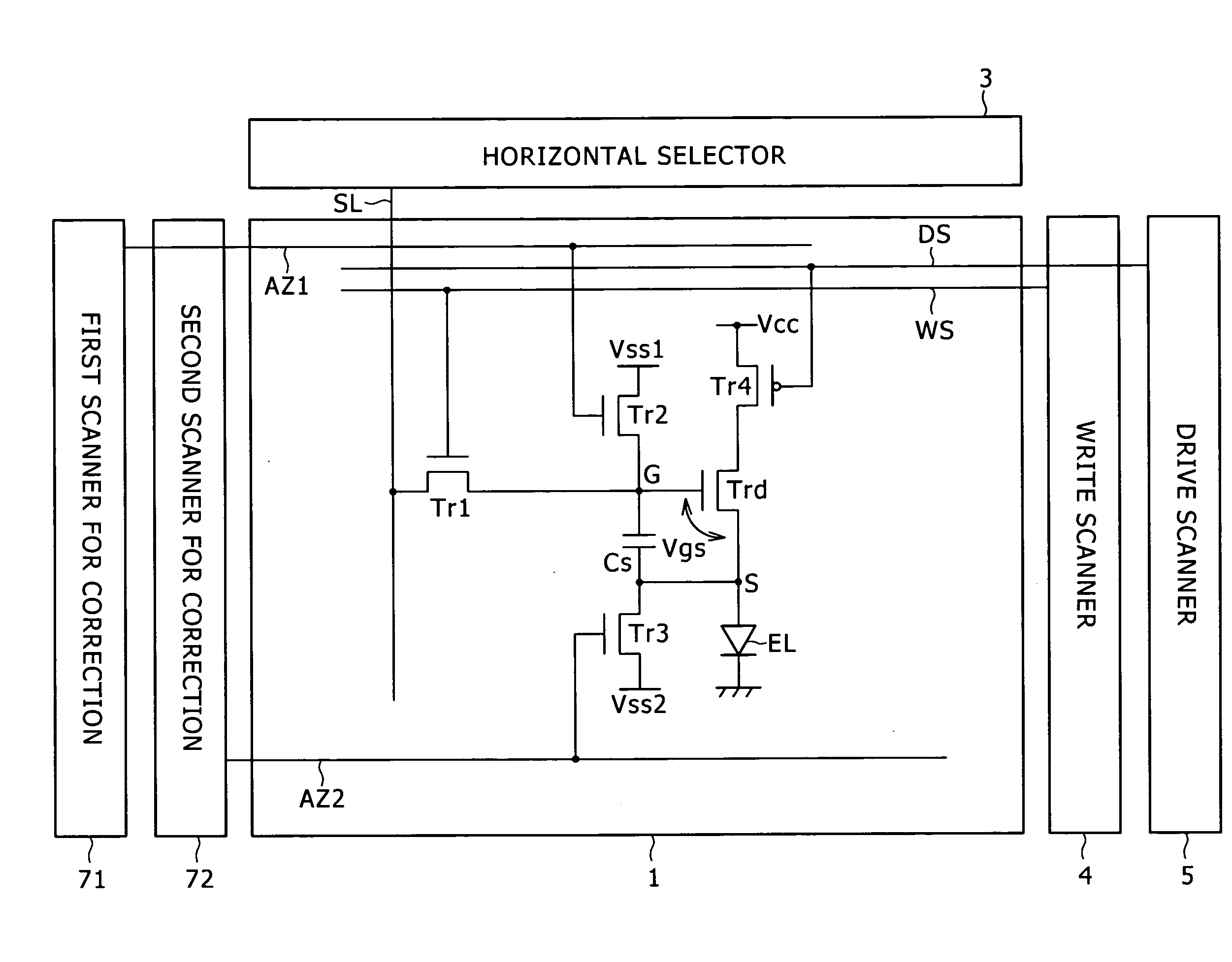
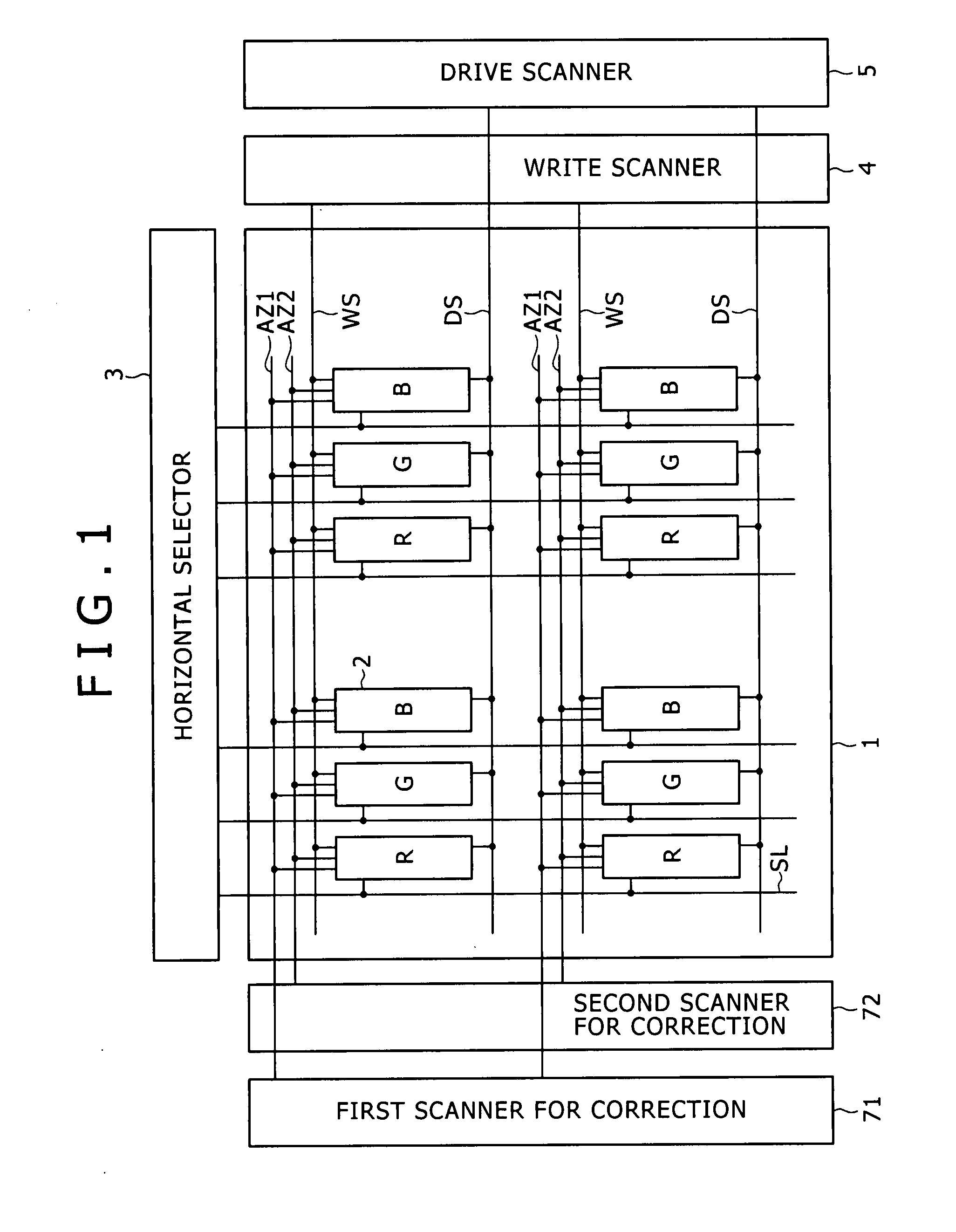
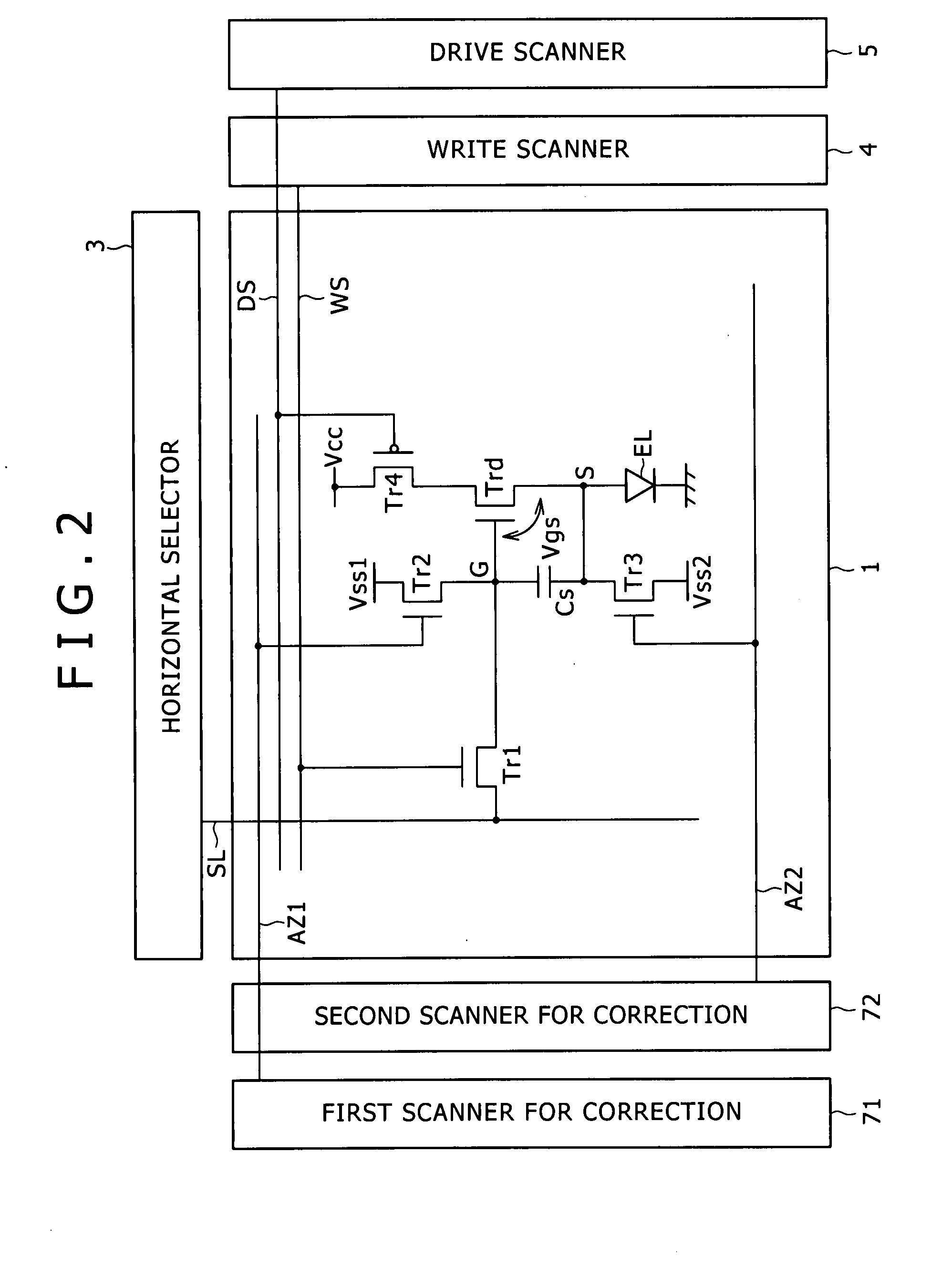
The present invention provides an image display device that reduces the number of scanning lines needed while still achieving uniformity of picture quality. The pixel circuit includes a sampling transistor, a drive transistor, and a light emitting element, and the scanner portion scans the pixel circuits every row by supplying control signals to the plurality of scanning lines, including main scanning lines, sub scanning lines, and scanning lines for correction. The pixel circuits are designed to cancel the dispersion of threshold voltages of the drive transistors, and the number of crossover laps among the scanning lines is reduced, resulting in improved yield and cost-down.

Problems solved by technology

The former involves such a problem that it is difficult to realize a large display device having a high definition although it is simple in constitution.

Method used


Image

  • Image display device
  • Image display device
  • Image display device

Examples


Embodiment Construction

[0034]Preferred embodiments of the present invention will be described in detail hereinafter with reference to the accompanying drawings. Firstly, a description will now be given with respect to an image display device according to a preceding development example as the base of the present invention (it may be hereinafter referred to as “a preceding development example”) with reference to FIG. 1. Since this preceding development example becomes the foundation of the present invention, and the greater part thereof overlaps in constitution the present invention, the preceding development example is now concretely described as a part of the present invention. As illustrated in FIG. 1, this image display device includes a pixel array portion 1, a scanner portion, and a signal portion as a basic constitution. The pixel array portion 1 includes a plurality of scanning lines WS, DS, AZ1 and AZ2 which are disposed every row, a signal line SL which is disposed every column, and pixel circuit...


PUM


Abstract

Herein disclosed an image display device including a pixel circuit array portion, a scanner portion, and a signal portion.

Description

CROSS REFERENCE TO RELATED APPLICATIONS[0001]The present invention contains subject matter related to Japanese Patent Application JP 2006-147537 filed in the Japanese Patent Office on May 29, 2006, the entire contents of which being incorporated herein by reference.BACKGROUND OF THE INVENTION[0002]1. Field of the Invention[0003]The present invention relates to an image display device in which a light emitting element such as an organic EL device is used in a pixel. Particularly, the invention relates to an active matrix type image display device for driving light emitting elements by scanning transistors formed in pixels, respectively. More particularly, the invention relates to a technique for reducing the number of plural scanning lines which are provided in rows of pixels.[0004]2. Description of the Related Art[0005]In an image display device such as a liquid crystal display device, a large number of liquid crystal elements are disposed in matrix and a transmission intensity or a...

Claims


Application Information

Patent Timeline
Patent Type & Authority Applications(United States)
IPC IPC(8): G09G3/30
CPCG09G3/3233G09G2300/0819G09G2320/043G09G2300/0861G09G2310/0262G09G2300/0842G09G3/20G09G3/30G09G3/32H05B33/12
Inventor YAMASHITA, JUNICHIUCHINO, KATSUHIDE
Owner SONY CORP
Learn More