
Two bits non volatile memory cells and method of operating the same

a non-volatile memory and two-bit technology, applied in the direction of electrical equipment, semiconductor devices, instruments, etc., can solve the problem of confined electrical components at a localized region, and achieve the effect of double non-volatile memory capacity

Inactive Publication Date: 2007-12-06
EMEMORY TECH INC
View PDF5 Cites 5 Cited by
  • Summary
  • Abstract
  • Description
  • Claims
  • Application Information

AI Technical Summary

Benefits of technology

[0008]An object of the present invention is to double non-volatile m

Problems solved by technology

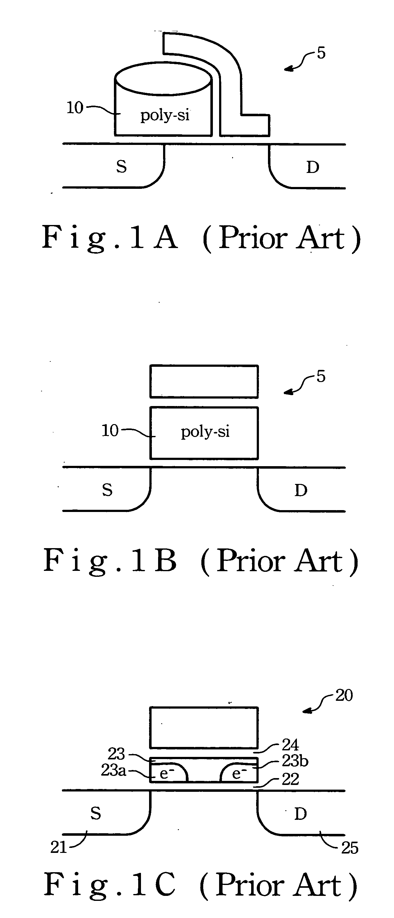
However, once electrons are captured or injected into the nitride layer 23, the electrons will be confined at a localized region due to their much lower mobility the nitride layer can provide.

Method used


Image

  • Two bits non volatile memory cells and method of operating the same
  • Two bits non volatile memory cells and method of operating the same
  • Two bits non volatile memory cells and method of operating the same

Examples


Embodiment Construction

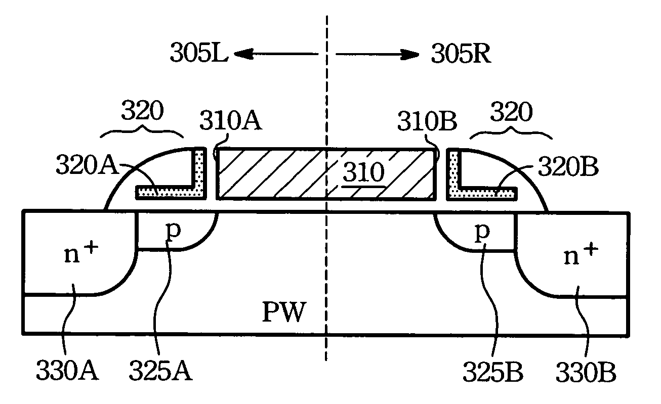
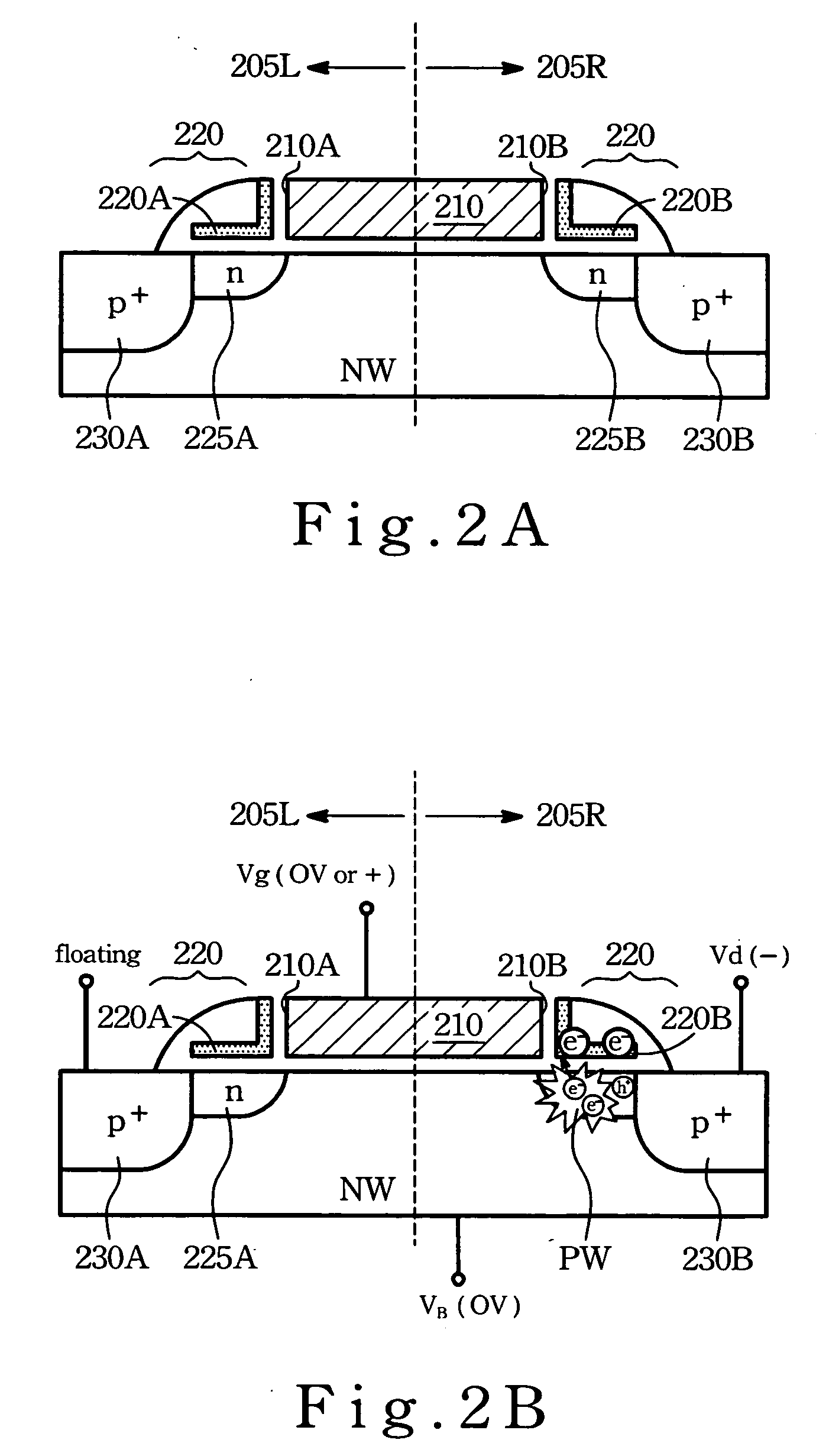
[0021]In a preferred embodiment, the present invention is to provide twin novel SONOS flash cells of which fabricating processes are completely compatible with those of analog CMOS (complementary metal oxide semiconductor transistor) processes. The two ONO spacers each having a nitride layer 220A (or 220B) served as a floating gate of a nonvolatile cell, are constructed at the sidewalls of a pMOS. The pMOS serves as a selected gate associated with individually voltages exerted at the source / drain and the body of the pMOS, a right floating gate, assuming it is formed at a drain side or a left floating gate formed at a source side can be appropriated selected and operated.

[0022]The pMOS based twin nonvolatile cells 205L, 205R are constructed in a n-well NW of a CMOS process. Please refer to FIG.2A, a cross-sectional view. It includes a selecting gate 210, two sidewalls 210A, 210B, ONO spacers 220 having, respectively, a L-mirror and a L shaped nitride layer,220A, 220B, a p+ doped sour...


PUM


Abstract

A twin non-volatile memory cell on unit device and method of operating the same are disclosed. The device is formed in the n-well and compatible with CMOS processes comprising a selecting gate, two ONO spacers, a p+ source / drain, and n extended source / drain. To program the cells, two strategies can be taken. One is by a band to band hot electron injection can be carried out. The other is by channel hot hole induced hot electron injection. To read the right cell of the twin nonvolatile cells, a reverse read is taken so as to shield the left cell. In the reading process, the biased on the selecting gate and the source electrode have to make sure the tapered main channel beneath selecting gate has its narrower end through the depletion boundary to connect the second channel beneath the extended source. To erase the datum in the selected cell, two approaching can be carried out. One is by FN erase, the other is by band to band induced hot hole injection.

Description

FIELD OF THE INVENTION[0001]The present invention relates to a nonvolatile memory structure, specifically, to a device having twin flash memory cells formed thereon and a method of operating the same.BACKGROUND OF THE INVENTION[0002]Flash disk is a kind of nonvolatile data storage apparatus. Once the data are stored, the lifetime of the data is at least over ten years without any electric energy to keep the data therein. To access data, it needs exerts voltages at individually electrodes only depends on what the operations are. By contrast, for hard disk apparatus, a stepping motor to carry magnetic read / write head flying on the magnetic disk is necessary. Hence, for flash disk, no mechanical vibrating problem is required to be considered. Furthermore, with fast progressing of semiconductor manufacture technique, an occupation volume of a flash disk is small significantly than that of a hard disk apparatus, for the same memory capacity is concerned. Consequently, the flash disk is a...

Claims


Application Information

Patent Timeline
IPC IPC(8): H01L29/788
CPCG11C16/0475H01L29/7923H01L29/66833H01L21/28282H01L29/40117
Inventor KING, YA-CHINLIN, CHRONG-JUNG
Owner EMEMORY TECH INC
Learn More