
Fin field effect transistor and method for forming the same

a field effect transistor and transistor technology, applied in transistors, semiconductor devices, electrical equipment, etc., can solve the problems of decreasing the effective length, and increasing the threshold voltage, so as to reduce the gidl and/or off current, the effect of expanding the effective length

Active Publication Date: 2007-12-06
SAMSUNG ELECTRONICS CO LTD
View PDF5 Cites 38 Cited by
  • Summary
  • Abstract
  • Description
  • Claims
  • Application Information

AI Technical Summary

Benefits of technology

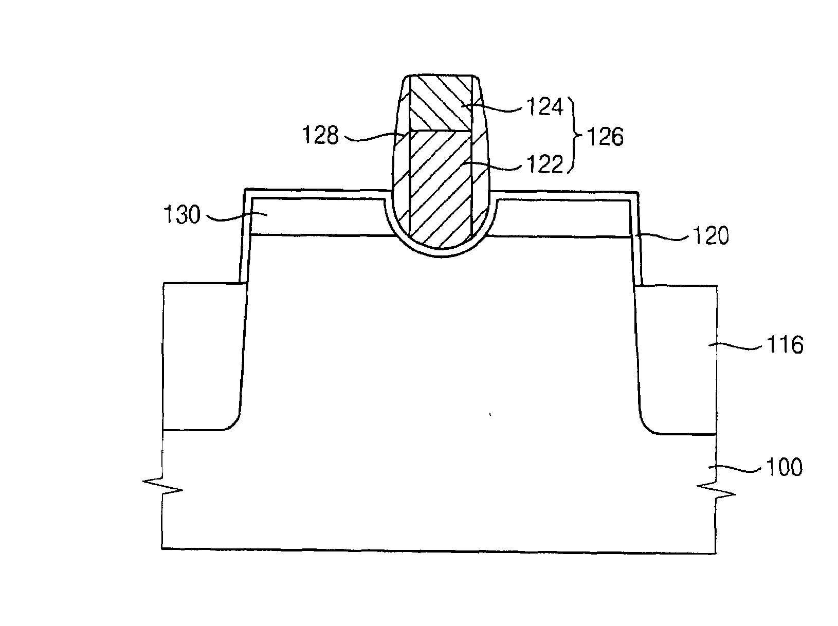
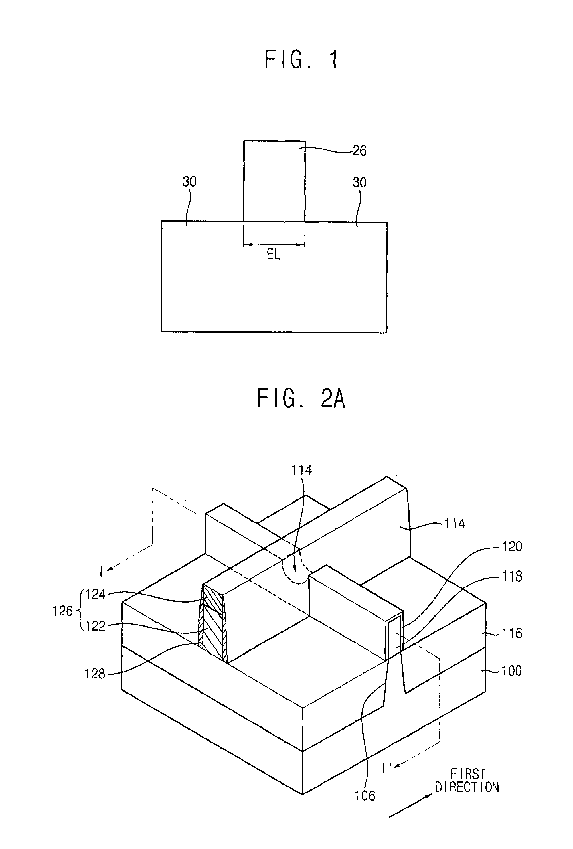
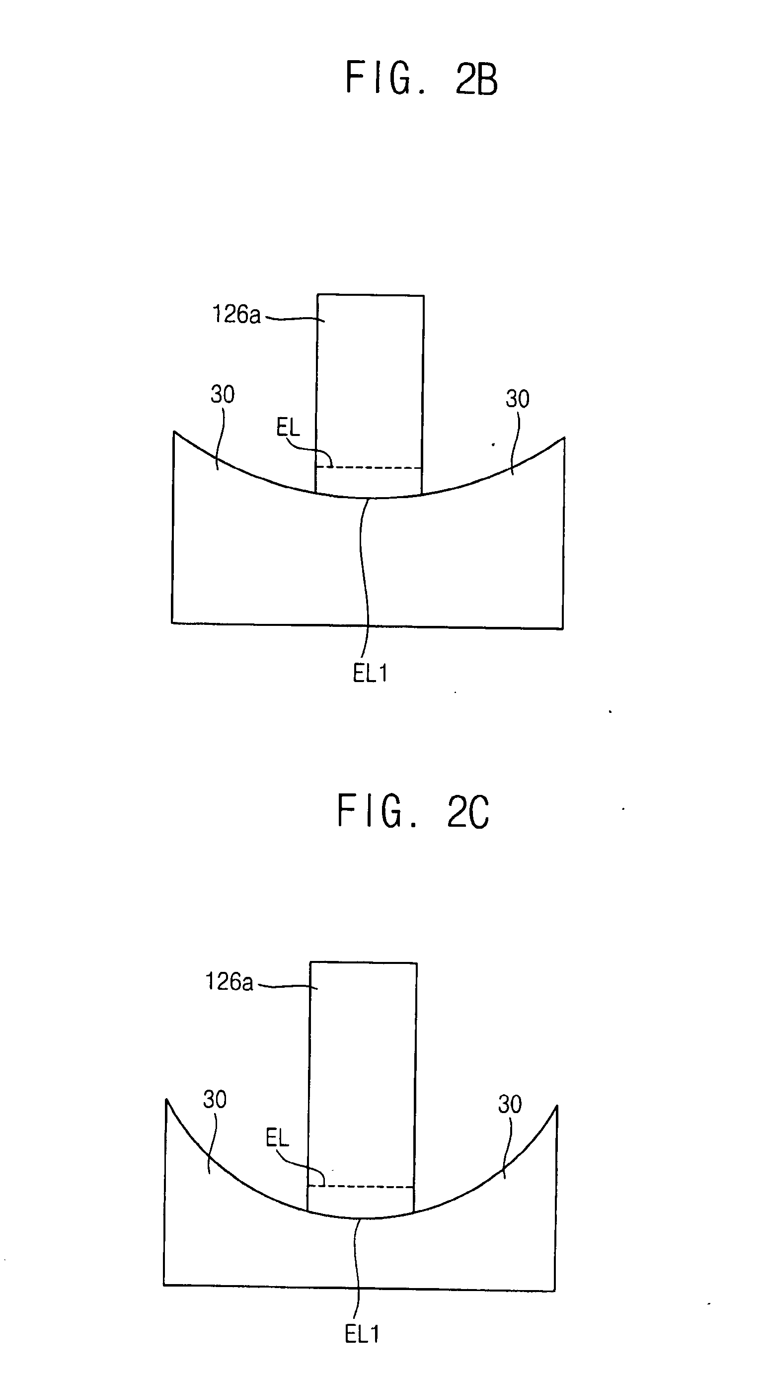
[0008]Example embodiments provide an elevated source / drain (S / D) structure. An elevated S / D structure may extend the effective length between the source and drain, therefore the GIDL and / or off current may be decreased.
[0018]In example embodiments, the recessed region may increase a surface area overlap between the at least one gate structure and the active fin.

Problems solved by technology

Further, scaling down the active size may include decreasing the channel width, which may increase a threshold voltage.
However, conventional FinFETs may also have problems.
Also, FinFETs may have a stronger GIDL (Gate-Induced Leakage) problem.

Method used


Image

  • Fin field effect transistor and method for forming the same
  • Fin field effect transistor and method for forming the same
  • Fin field effect transistor and method for forming the same

Examples


Embodiment Construction

[0044]Detailed example embodiments are disclosed herein. However, specific structural and / or functional details disclosed herein are merely representative for purposes of describing example embodiments. The claims may, however, may be embodied in many alternate forms and should not be construed as limited to only example embodiments set forth herein.

[0045]It will be understood that when a component is referred to as being “on,”“connected to” or “coupled to” another component, it can be directly on, connected to or coupled to the other component or intervening components may be present. In contrast, when a component is referred to as being “directly on,”“directly connected to” or “directly coupled to” another component, there are no intervening components present. As used herein, the term “and / or” includes any and all combinations of one or more of the associated listed items.

[0046]It will be understood that, although the terms first, second, third, etc. may be used herein to describ...


PUM


Abstract

Example embodiments are directed to a method of forming a field effect transistor (FET) and a field effect transistor (FET) including a source / drain pair that is elevated with respect to the corresponding gate structure.

Description

PRIORITY STATEMENT[0001]This application claims priority under 35 USC § 119 to Korean Patent Application No. 10-2006-43169 filed on May 13, 2006, the contents of which are herein incorporated by reference in their entirety for all purposes.BACKGROUND[0002]1. Field[0003]Example embodiments relate to field effect transistors (FETs), for example, to FETs and methods for manufacturing FETs.[0004]2. Description of the Related Art[0005]As the integration density of integrated circuit field effect transistors (FETs) continues to increase, the size of the active region and the channel length may continue to decrease. With the reduction in the channel length of the transistor, the influence of the source and / or drain upon the electric field or potential in the channel region may increase. This is called the “short channel effect”. Further, scaling down the active size may include decreasing the channel width, which may increase a threshold voltage. This is called the “narrow width effect”.[0...

Claims


Application Information

Patent Timeline
Patent Type & Authority Applications(United States)
IPC IPC(8): H01L29/78H01L21/336
CPCH01L29/66621H01L29/66795H01L29/792H01L29/7881H01L29/7851H01L21/18
Inventor KIM, KEUNNAMYOSHIDA, MAKOTO
Owner SAMSUNG ELECTRONICS CO LTD
Learn More