Boosted charge transfer circuit

a charge transfer circuit and boosted technology, applied in the field of boosted charge transfer circuits, can solve the problems of unacceptably long settling time of node b>4/b>, the effect of reducing the effect of the two error sources described above and sufficiently improving the performance of the boosted charge transfer circui

Active Publication Date: 2007-12-06
INTERSIL INC
View PDF29 Cites 39 Cited by
  • Summary
  • Abstract
  • Description
  • Claims
  • Application Information

AI Technical Summary

Benefits of technology

[0015] Embodiments of the present invention provide a charge-transfer circuit in which the effects of the two error sources described above are significantly reduced. In contrast to the passive charge transfer used in conventional BBDs, the charge transfer method of the present invention is termed “boosted”. The performance of a boosted charge-transfer circuit is sufficiently improved over that of the passive circuit that it makes high-speed, high-precision applications feasible.

Problems solved by technology

(In practical BBDs, VG is typically clocked rather than static, but it is not responsive to the charge being transferred.)
This passive charge transfer process is subject to two important error sources.
This declining current in turn results in a declining rate of charging of node 4.
Moreover, with practical circuit values, the settling time of node 4 is unacceptably long for high-speed circuit operation.
Passive charge-transfer is thus both slow and non-linear; in many applications these limitations degrade speed and accuracy unacceptably.

Method used


Image

  • Boosted charge transfer circuit
  • Boosted charge transfer circuit
  • Boosted charge transfer circuit

Examples


Embodiment Construction

[0031] A description of preferred embodiments of the invention follows.

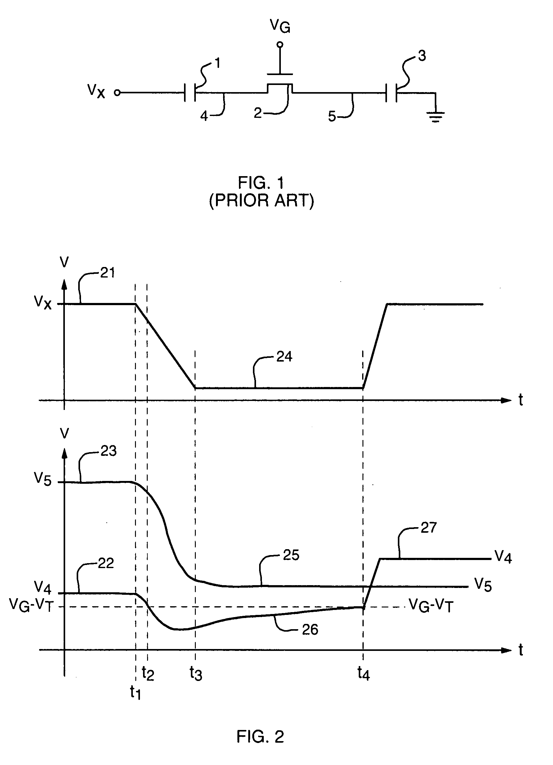
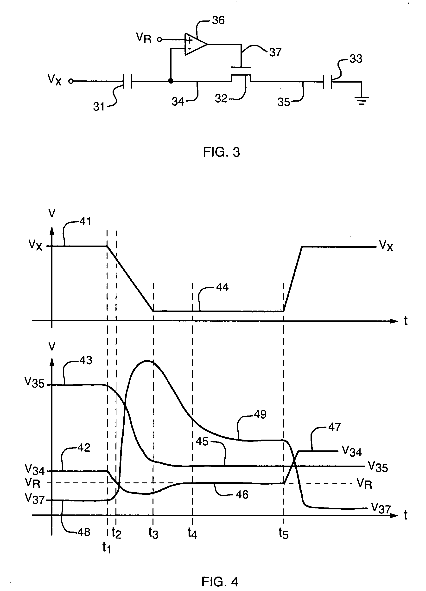
[0032] The present invention provides a charge-transfer circuit in which the effects of the two error sources described above are significantly reduced. In contrast to the passive charge transfer used in conventional BBDs, the charge transfer method of the present invention is termed “boosted”. The performance of a boosted charge-transfer circuit is sufficiently improved over that of the passive circuit that it makes high-speed, high-precision applications feasible. This boosted charge-transfer technique can be understood with the aid of FIGS. 3 and 4, which illustrate the basic features of its operation.

[0033] The elements of FIG. 3 are the same as similarly-identified elements of FIG. 1, except for the addition of amplifier 36 and its reference voltage VR, and the omission of voltage VG. Capacitor 31 in FIG. 3 corresponds to capacitor 1 in FIG. 1, node 34 to node 4, etc. The added amplifier 36 is the unique f...


PUM


Abstract

A charge transfer circuit, such as a charge coupled device or other bucket brigade device, which incorporates an amplifier to assist with charge transfer.

Description

RELATED APPLICATION [0001] This application claims the benefit of U.S. Provisional Application No. 60 / 809,485, filed on May 31, 2006. The entire teachings of the above application are incorporated herein by reference.BACKGROUND OF THE INVENTION [0002] In charge-domain signal-processing circuits, signals are represented as charge packets. These charge packets are stored, transferred from one storage location to another, and otherwise processed to carry out specific signal-processing functions. Charge packets are capable of representing analog quantities, with the charge-packet size in coulombs being proportional to the signal represented. Charge-domain operations such as charge-transfer are driven by ‘clock’ voltages, providing discrete-time processing. Thus, charge-domain circuits provide analog, discrete-time signal-processing capability. [0003] Charge-domain circuits are implemented as charge-coupled devices (CCDs), as Metal Oxide Semiconductor (MOS) bucket-brigade devices (BBDs),...

Claims


Application Information

Patent Timeline
Patent Type & Authority Applications(United States)
IPC IPC(8): H04N5/335G11C7/10G11C19/28
CPCG11C19/285G11C19/186G11C7/10G11C5/14
Inventor ANTHONY, MICHAEL P.
Owner INTERSIL INC
Why Eureka
Try Eureka