Method And Apparatus For Self-Referenced Wafer Stage Positional Error Mapping

a technology of positional error mapping and self-reference, which is applied in the field of manufacturing processes requiring lithography, can solve the problems of reducing the feature size of the device, affecting the performance of photolithographic exposure tools or machines, and pushed to performance limits, etc., and achieves the effect of being easily employed

Inactive Publication Date: 2007-12-06
LITEL INSTR
View PDF35 Cites 17 Cited by
  • Summary
  • Abstract
  • Description
  • Claims
  • Application Information

AI Technical Summary

Benefits of technology

[0037] A wafer stage error map is created using standard overlay targets and a special numerical algorithm. A reticle consisting of a 2-dimensional array of standard overlay targets is exposed several times onto a photoresist coated silicon wafer using a photolithographic projection tool (machine). Next, the overlay targets are measured for placement error using a conventional overlay metrology tool. The resulting overlay error data are then fed into a software program that generates a 2-dimensional wafer stage error map. Most importantly, the method determines wafer stage overlay error, namely, wafer stage distortion and yaw, excluding, total or average translation, and rotation. In summary, the projected field of the overlay reticle is used as a rigid 2-dimensional ruler, and the stage errors are determined in detail with respect to the dimensions of a single projected image field. The method described above does not require the use of a special reference stepper or golden wafer to obtain the wafer stage contributions to placement error. The preferred embodiment is both self-consistent and self-referenced thus reducing the need of cross calibration between different exposure tool sets to a bare minimum. In addition, variations of the preferred embodiment can be used to calculate stage repeatability or precision using standard statistical methods. The ability to determine true stage distortion and yaw without cross calibration or reference to other stepper systems allows the user to more accurately model additional sources of placement error. The method described above can be adjusted for accuracy by simply adjusting the number of measurements made of the alignment attributes or overlay targets. The invention requires exposing and printing an array of fields in a periodic interlocking pattern across the wafer. Next, the resulting overlay target patterns can be measured for overlay error using a standard commercially available optical overlay metrology tool. Next, the distortion and yaw components of stage overlay error are computed using a special algorithm. The method and apparatus form a methodology that can be modified slightly to achieve varying degrees of overall accuracy. The following procedure can be easily implemented in a modern semiconductor manufacturing facility.
[0041] The fact that the preferred method utilizes a high precision overlay metrology tool for local measurements and extracts the overlay error associated with wafer stage distortion and yaw in a unique way means that the technique is readily employed in semiconductor manufacturing facilities (fabs). In addition, this invention can be used in conjunction with traditional overlay techniques to better understand, model and correct pattern placement errors. Additional applications of the above outlined procedure include: improved lithographic simulation using conventional optical modeling software, advanced process control in the form of feedback loops that automatically adjust the wafer stage for optimum performance, and finally, wafer stage correction algorithms that compensate for distortion and yaw effects. The software algorithm and apparatus form a self-referenced methodology that does not require a special set of overlay calibration wafers, a special reference stepper tool or assumptions concerning the magnitude of distortion and yaw overlay errors.

Problems solved by technology

Increasing device densities, decreasing device feature sizes and greater overall device size conspire to make pattern overlay one of the most important performance issues during the semiconductor manufacturing process.
Overlay error is typically, although not exclusively, measured with an optical overlay metrology tool.
Intra-field overlay errors are typically related to lens aberrations and reticle alignment.
Today, these photolithographic exposure tools or machines are pushed to performance limits.
There are several problems associated with this technique.
First, as noted above, the technique does not yield the unique wafer stage overlay error; it only provides a relative measure of all components.
To obtain the relative stage error between two machines, the inter-field errors so determined must be subtracted from one another, which results in increasing the noise in the determination of stage error.
Second, the models used to calculate the systematic inter-field error usually do not account for the stage error associated with distortion and yaw.
They are typically limited to translation, rotation, orthogonality and x and y scale errors.
Problems with this technique are: the systematic (repeatable) and random grid errors on the reference machine (the machine used for creating the reference wafers) are permanently recorded as half (inner or outer box) of our factory wide metrology standard.
Furthermore, reference machine instabilities over time lead to a drift or error in the factory wide standard represented by the reference machine.
Yet another problem with this technique is that because it utilizes full size projected fields to determine the inter-field errors, it does not work with partially exposed fields as illustrated in FIG. 44.
The ability to include partially exposed fields is important since product wafers typically contain multiple die within an exposure field, and therefore the inter-field error of partially exposed fields is important since it directly affects the edge die overlay error.
Unfortunately, this technique cannot be applied to photolithographic exposure tools (machines) since the wafer position (artifact) typically cannot be placed on the wafer chuck in a position significantly (>=1 mm) shifted from the nominal position.
In some machines, such a shift may be possible with extraordinary effort on the part of the maintenance engineer, but such a procedure is completely unsuitable in ordinary production use.
Another disadvantage of this technique is that it does not measure the stage yaw.
Yet another disadvantage of the aforementioned technique is that the measurement process utilizes the production machine itself to perform the metrology; this means there is less time available for making product on that machine.
Yet another disadvantage of this technique is it does not allow us measure stage error for partially exposed fields.
In addition, there is a need to measure the wafer stage positioned error in a production environment by the day to day operating personnel.

Method used


Image

  • Method And Apparatus For Self-Referenced Wafer Stage Positional Error Mapping
  • Method And Apparatus For Self-Referenced Wafer Stage Positional Error Mapping
  • Method And Apparatus For Self-Referenced Wafer Stage Positional Error Mapping

Examples


1st alternate embodiment

1st Alternate Embodiment

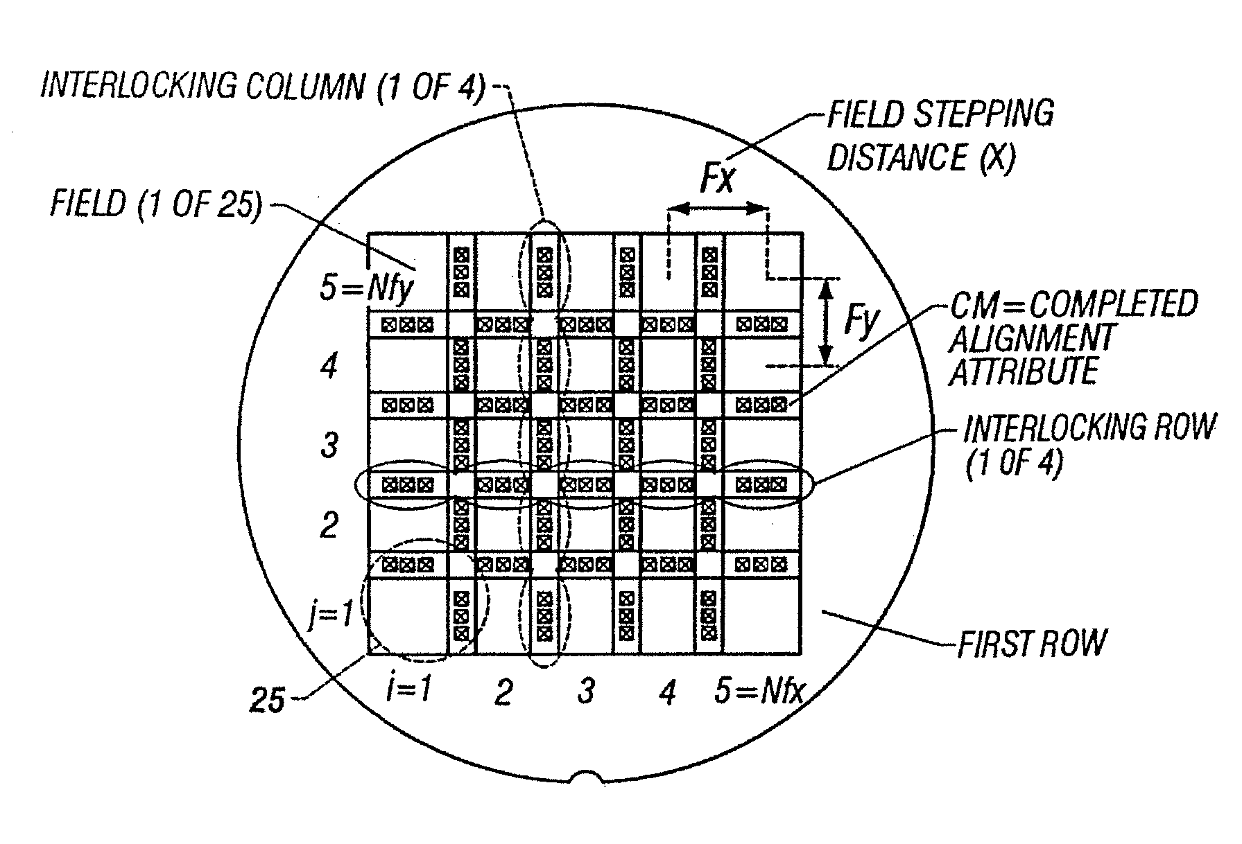
[0150] Thus far, the preferred embodiment has been used to extract the components of overlay error associated with wafer stage distortion and yaw using a single wafer to fully account for all repeatable and non-repeatable effects of wafer stage placement error. To extract the repeatable effects of wafer stage placement error using the method of the preferred embodiment we must expose a number, N, of wafers on the same machine and average the resulting set of N wafer stage errors. We now describe a variation of the preferred embodiment that allows the user to extract the repeatable components of overlay error associated with wafer stage distortion and stage yaw in the presence of wafer stage non-repeatability using only one or a minimum number of wafers.

[0151] First, the overlay target reticle and photoresist coated wafer are loaded into the projection lithography tool (machine) and properly aligned as described in the preferred embodiment. Next, the machine ...

2nd alternate embodiment

2nd Alternate Embodiment

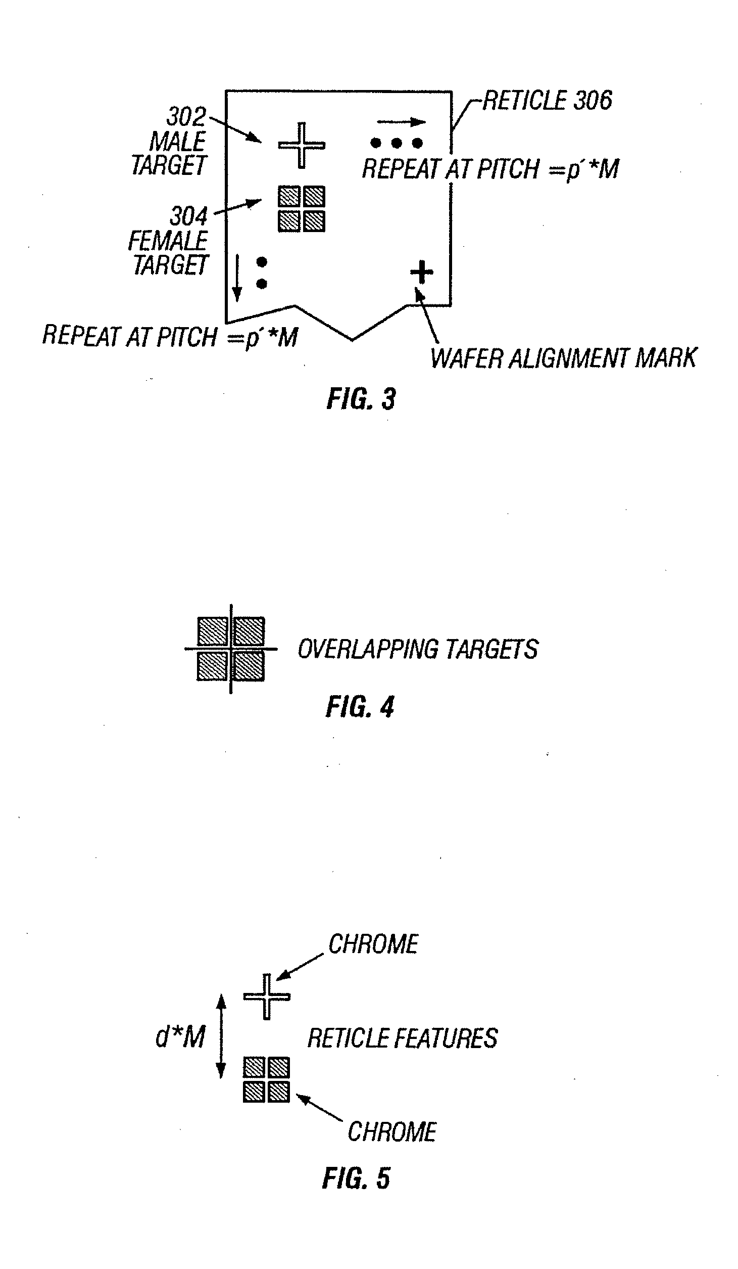
[0153] In this embodiment, see flow diagram FIG. 17, we also perform multiple exposure sequences to average out the effect of machine random stage error but now we provide the overlay reticle of FIG. 21A with a partially reflecting dielectric coating either on its top (non-chrome) or possibly bottom surface (chrome coated or machine optical object plane), as shown in FIG. 21B. A 95% reflecting dielectric coating applied to the overlay reticle means that if we do 40 exposure sequences at a dose of Eo each; the net effect is to expose the wafer with a dose of 2*Eo and to have effectively averaged over 20 or more exposures.

[0154] An advantage of this technique is that we are will not as limited by the machine's ability to do sub-Eo exposures. A further advantage of this technique is that since the exposure doses can be made at the same dose as used in production runs, the dynamics of the stage movement during the measurement sequence will be the same and theref...


PUM

PropertyMeasurementUnit
timeaaaaaaaaaa
optical transmissionaaaaaaaaaa
dielectricaaaaaaaaaa

Abstract

A wafer stage overlay error map is created using standard overlay targets and a special numerical algorithm. A reticle including a 2-dimensional array of standard overlay targets is exposed several times onto a photoresist coated silicon wafer using a photolithographic exposure tool. After exposure, the overlay targets are measured for placement error using a conventional overlay metrology tool. The resulting overlay error data is then supplied to a software program that generates a 2-dimensional wafer stage distortion and yaw overlay error map.

Description

REFERENCE TO PRIORITY DOCUMENT [0001] This application is a continuation of U.S. application Ser. No. 10 / 775,718 filed on Feb. 9, 2004, which is a continuation of U.S. application Ser. No. 09 / 891,699 filed Jun. 26, 2001, which claims priority to U.S. Provisional Application Ser. No. 60 / 254,413 filed Dec. 8, 2000. These applications are incorporated by reference in their entirety herein.BACKGROUND OF THE INVENTION [0002] 1. Field of the Invention [0003] The present invention relates generally to manufacturing processes requiring lithography and more particularly to characterizing and monitoring the inter-field errors of semiconductor wafer stages. [0004] 2. Description of the Related Art [0005] Today's lithographic processing requires ever tighter layer-to-layer overlay tolerances to meet device performance requirements. Overlay registration is defined as the translational error that exists between features exposed layer to layer in the vertical fabrication process of semiconductor d...

Claims


Application Information

Patent Timeline
Patent Type & Authority Applications(United States)
IPC IPC(8): G03B27/68G03F7/20
CPCG03F7/70558G03F7/70633G03F7/70616G03F7/70591
Inventor SMITH, ADLAIMCARTHUR, BRUCEHUNTER, ROBERT JR.
Owner LITEL INSTR
Why Eureka
Try Eureka