Methods and systems for designing high resolution analog to digital converters

a converter and high-resolution technology, applied in transmission systems, analogue/digital conversion, instruments, etc., can solve problems such as gain error and reference voltage error, reducing the performance of adc, and reducing the performance of adc, and achieve high-resolution effects

Inactive Publication Date: 2007-12-13
COSMIC CIRCUITS PRIVATE LIMITED
View PDF21 Cites 6 Cited by
  • Summary
  • Abstract
  • Description
  • Claims
  • Application Information

AI Technical Summary

Benefits of technology

[0018] Embodiments of the invention described herein provide methods and systems for designing a high resolution ADC by eliminating the errors in the ADC stages. An error correction architecture and method of the embodiments of the invention eliminate ...

Problems solved by technology

These errors are the key reason for reducing the performance of the ADC.
Mainly there are two types of errors which reduce the performance of the ADC, namely gain error and reference voltage error.
If the gain of the residue amplifier of a stage varies from the desired gain, there is a gain error in the residue amplifier which affects the residue value output of that particular stage.
Error in residue value results in erroneous decisio...

Method used


Image

  • Methods and systems for designing high resolution analog to digital converters
  • Methods and systems for designing high resolution analog to digital converters
  • Methods and systems for designing high resolution analog to digital converters

Examples


Embodiment Construction

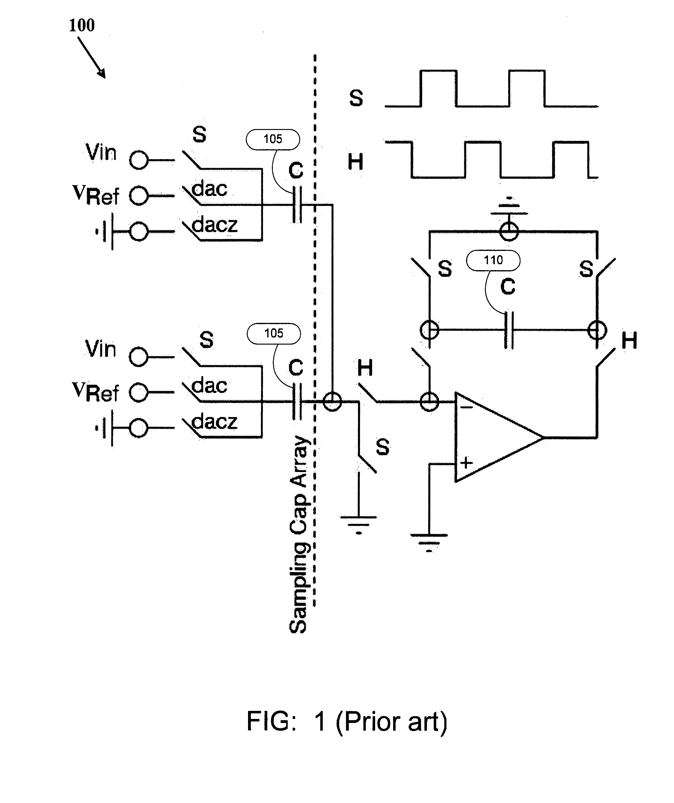
[0032]FIG. 1 illustrates a stage of a pipelined ADC according to the prior art 100.

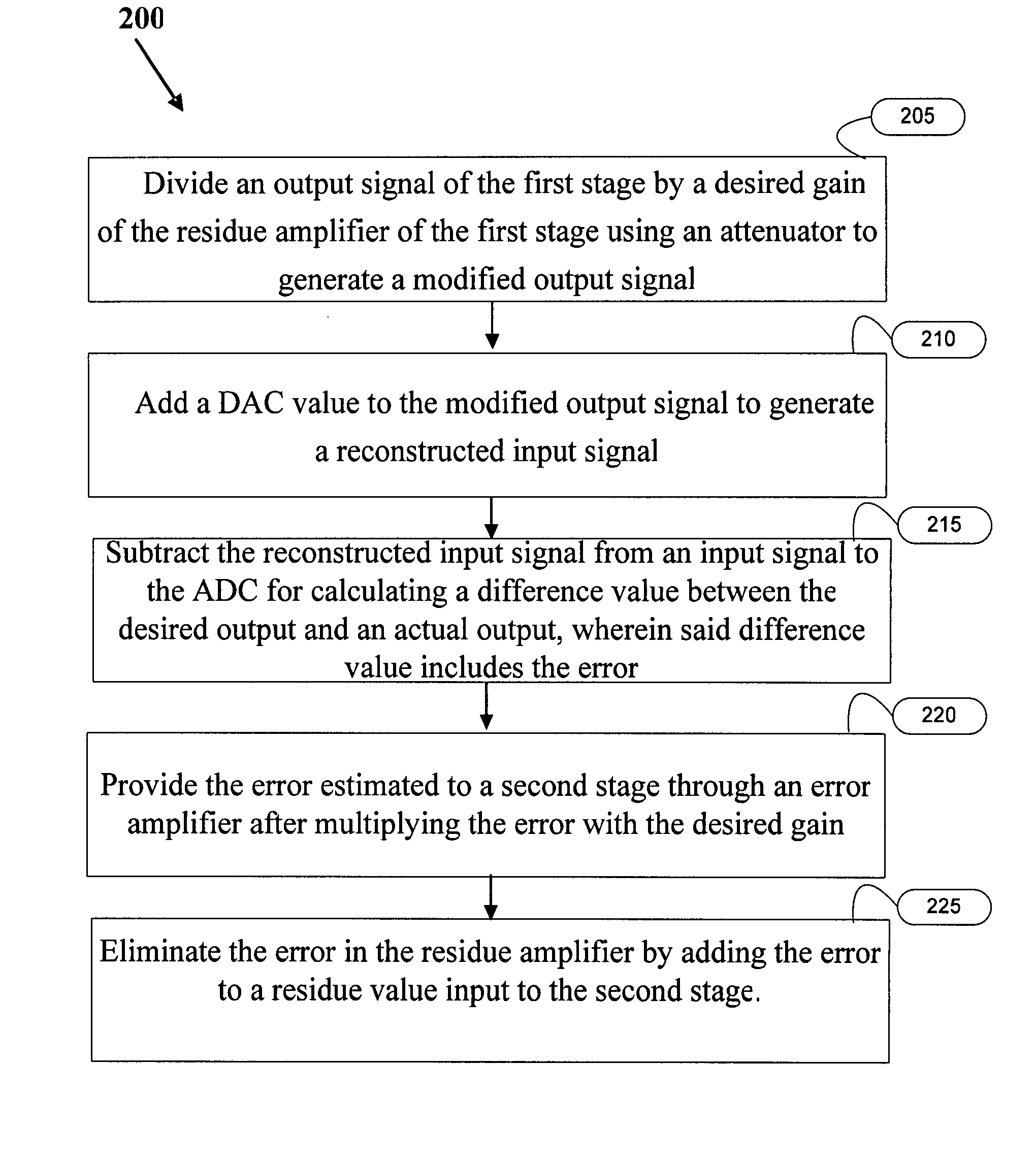
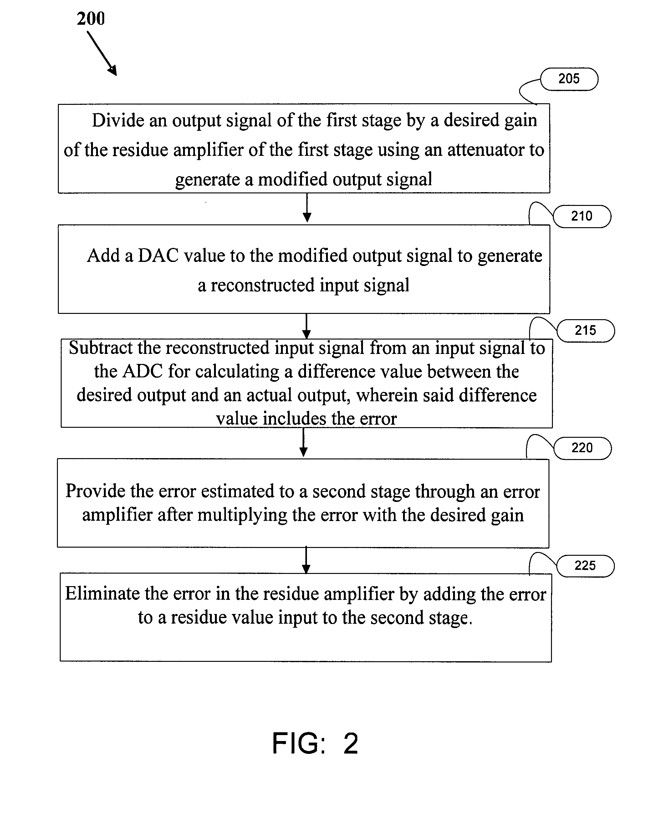
[0033]FIG. 2 is flow diagram illustrating the steps in the method 200 for error correction in an ADC according to an embodiment of the invention. The error caused by a residue amplifier of a stage of the ADC is estimated while ADC is performing the analog to digital conversion, and is forwarded and corrected in the next stage. The error correction method uses an analog feed-forward approach where the error calculated is propagated and corrected in the analog domain at the later stages. Step 205 divides an output signal of the first stage by a desired gain of the residue amplifier of the first stage using an attenuator and generates a modified output signal. Step 210 adds the DAC value to the modified output signal and generates a reconstructed input signal. Step 215 subtracts the reconstructed input signal from an input signal to the ADC for calculating a difference value between the desired output a...


PUM


Abstract

Methods and systems for designing a high resolution ADC by eliminating the errors in the ADC stages. An error correction architecture and method of the embodiments of the invention eliminate the gain error and settling error of the residue amplifier in a pipelined ADC stage. A reference voltage error correction architecture and method of the embodiments of the invention eliminate the reference voltage error due to the sampling action in the ADC. The gain error correction method calculates the gain error using an error amplifier and eliminates the gain error at a later stage of the ADC. The reference voltage error correction method calculates the reference voltage error using an ideal reference voltage and corrects the error at a later stage of the ADC. The constraints of gain and settling of the residue amplifier is significantly reduced using the embodiments of the invention.

Description

CROSS-REFERENCE TO RELATED APPLICATIONS [0001] This application claims priority to Indian Provisional Patent Application No. 1006 / CHE / 2006, filed Jun. 9, 2006, and Indian Non-Provisional Patent Application No. E / 2 / 116 / 207, filed Jun. 8, 2007, which are incorporated herein by reference. BACKGROUND [0002] 1. Technical Field [0003] Embodiments of the invention relate generally to Analog to Digital Converters (ADCs) and more particularly to methods and systems for designing high resolution ADCs. [0004] 2. Discussion of Prior Art [0005] Analog to Digital Converters (ADCs) serve to translate a given analog input signal (over a given range of potential signal values) into a corresponding digital signal. The prior art is replete with a host of different types of ADC architectures. They include, for example, flash architecture, pipelined architecture, successive approximation architecture and sigma delta architecture. [0006] A pipelined ADC divides an analog-to-digital conversion task into s...

Claims


Application Information

Patent Timeline
IPC IPC(8): H03M1/12
CPCH03M1/168H03M1/0604
Inventor EASWARAN, PRAKASHBHATTACHARYA, PRASUN KALIT.S, VENKATESH
Owner COSMIC CIRCUITS PRIVATE LIMITED
Why Eureka
Try Eureka