

Photoelectric conversion layer stack type solid-state imaging device
a technology of photoelectric conversion and stacking, which is applied in the direction of television system scanning details, radioation control devices, television systems, etc., can solve the problems of reducing image quality, reducing image quality, and unable to read complete color signals, etc., and achieves low image quality and afterimages. high degree
- Summary
- Abstract
- Description
- Claims
- Application Information
AI Technical Summary
Benefits of technology
Problems solved by technology
Method used
Image

Examples
embodiment 1
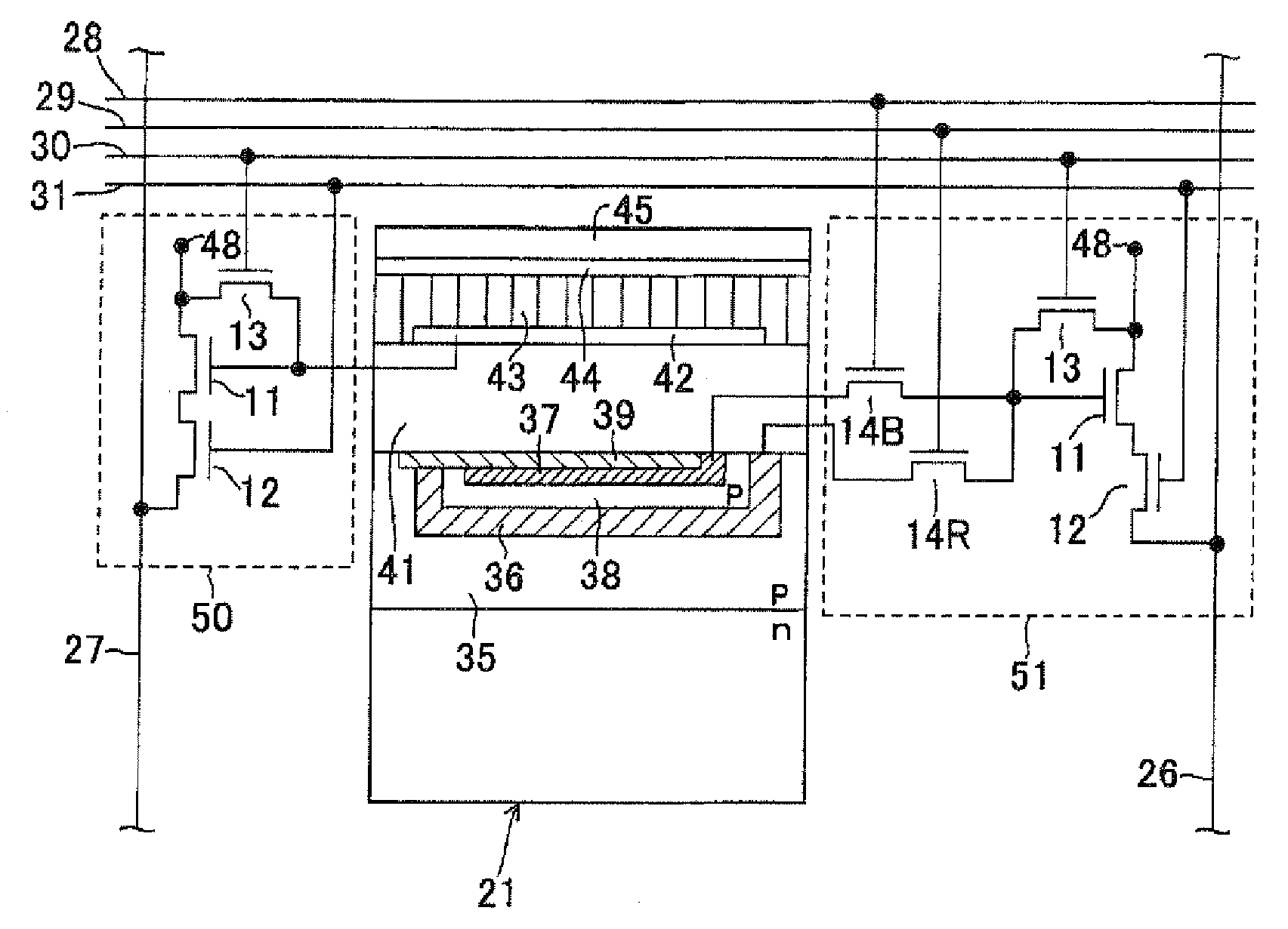
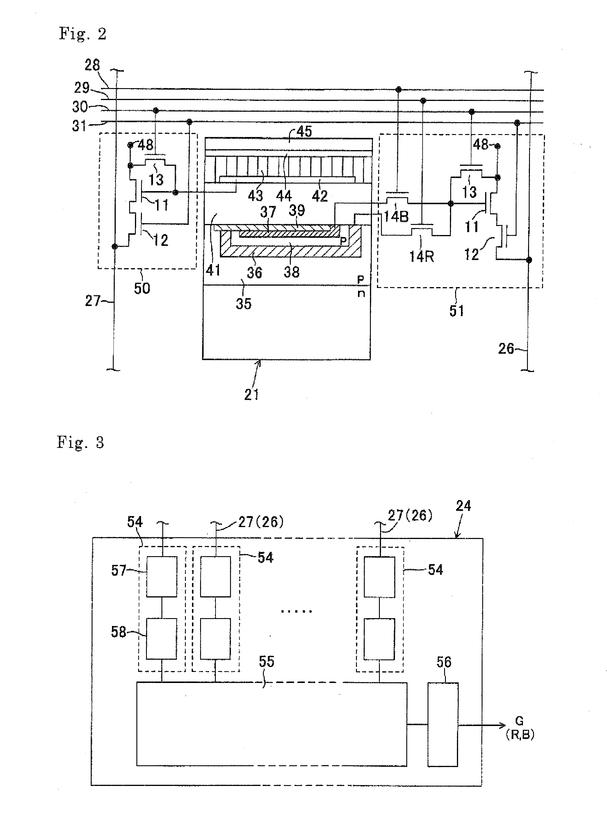
[0074]FIG. 1 schematically shows the surface of a photoelectric conversion layer stack type color solid-state imaging device according to a first embodiment of the invention. In the photoelectric conversion layer stack type color solid-state imaging device 20, plural unit pixels 22 are arranged in square lattice form. Output signal processing sections 23 and 24 each including a row-direction scanning reading section are disposed adjacent to the top and bottom sidelines of the semiconductor substrate 21, respectively. A column-direction scanning control section 25 is disposed adjacent to the left sideline of the semiconductor substrate 21. In this embodiment, the output signal processing section 23 is in charge of red (R) signals and blue (3) signals and the output signal processing section 24 is in charge of green (G) signals.
[0075]The unit pixels 22 are connected to the output signal processing section 23 via column signal lines 26 and connected to the output signal processing sect...
embodiment 2
[0114]FIG. 4 schematically shows the surface of a photoelectric conversion layer stack type color solid-state imaging device 60 according to a second embodiment of the invention. The same components as in the first embodiment will be given the same symbols as in the first embodiment and will not be described.
[0115]This embodiment is characterized in that the two output signal processing sections 23 and 24 of the first embodiment shown in FIG. 1 are communized into a single output signal processing circuit 61. The sectional structure of each unit pixel 22 and the circuit configurations of the signal reading circuits 50 and 51 are the same as in the first embodiment (see FIG. 2). Each unit pixel 22 is connected to the output signal processing circuit 61 via column signal lines 26 and 27.
[0116]FIG. 5 shows the configuration of the output signal processing circuit 61 according to this embodiment. In this embodiment, to connect, to each single correlation double sampling circuit 54, the ...
embodiment 3
[0124]FIG. 6 shows the configuration of an important part of an output signal processing section of a photoelectric conversion layer stack type color solid-state imaging device according to a third embodiment of the invention The entire configuration, the sectional structure, etc. of the photoelectric conversion layer stack type color solid-state imaging device according to this embodiment are the same as those of the imaging device according to the second embodiment (see FIGS. 4 and 2) and hence will not be described in detail.
[0125]Each analog circuit unit of the output signal processing section of this embodiment is composed of the switch circuit 62 that was described above with reference to FIG. 5 and a sampling circuit 54 which is composed of a clamp circuit 57 and a sample-and-hold circuit 58. And each analog circuit unit is characterized in that a switch circuit 63 is provided in a bypass route of the clamp circuit 57 and makes effective or breaks the bypass route.
[0126]When ...
PUM
 Abstract
Description
Claims
Application Information