Production of an improved color filter on a microelectronic imaging device comprising a cavity

Active Publication Date: 2007-12-13
STMICROELECTRONICS SRL
View PDF6 Cites 1 Cited by
  • Summary
  • Abstract
  • Description
  • Claims
  • Application Information

AI Technical Summary

Benefits of technology

[0010]In one possible embodiment of the method, a zone based on the first material or the second material or the third material, may be produced between the first group and the second group. This may allow the loss of adhesion phenomena of the filtering elements close to the vertical walls of the cavity to be limited.
[0011]In one variant, a zone based on a transparent material that is different from the first, second and third materials, may be produced between the first group and the second group. This may also allow the loss of adhesion phenomena of the filtering elements close to the vertical walls of the cavity to be limited.

Problems solved by technology

This can lead to an incorrect definition of the filtering elements located at the periphery of the matrix.
In this case especially, the formation of the color filter, and, in particular, the photolithographic method which permits the blocks of resin to be defined raises a problem in that it is difficult to obtain resin patterns with correct definition both inside and outside of the cavity at the same time.
Furthermore, if one favors obtaining resin patterns with the correct definition inside of the cavity, a phenomenon of the resin outside of the cavity losing adhesion may occur.

Method used


Image

  • Production of an improved color filter on a microelectronic imaging device comprising a cavity
  • Production of an improved color filter on a microelectronic imaging device comprising a cavity
  • Production of an improved color filter on a microelectronic imaging device comprising a cavity

Examples


Embodiment Construction

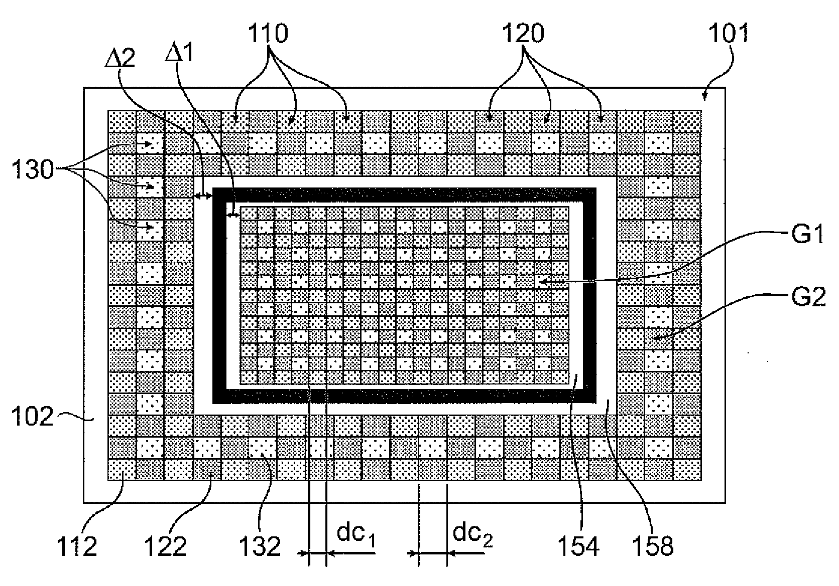
[0025]A microelectronic device equipped with a color filter made in thin layers, is illustrated in a top view in FIG. 1 and in a cross sectional view in FIG. 5H. This microelectronic device may be, for example, an imaging device or image sensor. The color filter 101 comprises a plurality of filtering elements formed on a transparent insulating layer 102, for example, SiO2 and / or Si3N4 based. The filter 101 comprises filtering elements of a first type 110, and capable of filtering a first range of wavelengths of the visible luminous spectrum, for example, wavelengths greater than 550 nm. The filtering elements of the first type 110 may be, for example, in the form of blocks based on a first material 112, such as a polymer or a resin, colored or equipped with colored pigments, for example, metallic pigments. The first material 112 may be, for example, a blue resin or comprising blue pigments. The filter 101 also comprises filtering elements of a second type 120, capable of filtering a...


PUM


Abstract

A microelectronic device includes a color filter equipped with a plurality of filtering elements, including several filtering elements. The device includes at least one first zone located inside a cavity and includes a first group of filtering elements having a first critical dimension, and at least one second zone at the periphery of the cavity, including a second group of filtering elements having a second critical dimension that is different from the first critical dimension.

Description

FIELD OF THE INVENTION[0001]The invention relates to the field of microelectronics, and, more particularly, to that of microelectronic devices, such as imaging devices or image sensors, equipped with photoelectric detector components provided to produce a photoelectric current by absorption of incidental visible luminous radiation.BACKGROUND OF THE INVENTION[0002]A microelectronic imaging device or image sensor is generally formed by a matrix of pixels and of at least one electronic control circuit formed around the matrix. Each pixel comprises at least one photoelectric detector, for example, a photodiode or a phototransistor, provided to convert the energy of the incidental photons on the pixel into electron-hole pairs. The matrix of pixels also called the “active matrix” may be especially covered with an insulating layer and a trichromatic or three color filter formed on this insulating layer. The color filter is formed by colored filtering elements, respectively capable of filte...

Claims


Application Information

Patent Timeline
IPC IPC(8): H01L21/00
CPCH01L27/14603H01L27/14685H01L27/14627H01L27/14621
Inventor HOTELLIER, NICOLASFELLOUS, CYRILCOWACHE, CHRISTOPHESANCHEZ, YANNICK
Owner STMICROELECTRONICS SRL
Why Eureka
Try Eureka