Thin substrate processing device

a technology of processing device and thin substrate, which is applied in the direction of vacuum evaporation coating, coating, electric discharge tube, etc., can solve the problem of limited temperature rise of thin substrate, and achieve the effect of enhancing the cooling effect of thin substra

Active Publication Date: 2019-08-06
ULVAC INC
View PDF26 Cites 0 Cited by
  • Summary
  • Abstract
  • Description
  • Claims
  • Application Information

AI Technical Summary

Benefits of technology

[0010]According to this configuration, transportation of the thin substrate when the thin substrate and the cooling unit are in contact with each other can be limited so that damaging of the thin substrate and the cooling unit can be limited.
[0016]According to this configuration, the thin substrate is reversely sputtered when the surface of the target is covered by the shutter. Therefore, even when a film formation processing unit and a reverse sputtering unit are set in the same vacuum chamber, adhesion of the grains discharged from the thin substrate by the cleaning (reverse sputtering) of the film substrate to the surface of the target can be limited. This reduces the grains released from the thin substrate that are included in the sputtering grains discharged from the target.
[0019]As a result of research into the conditions of performing reverse sputtering on the thin substrate, the inventors of the present application have found that when the frequency of the voltage applied to the thin substrate is higher than or equal to 1 MHz and lower than or equal to 6 MHz, the speed of reversely sputtering the thin substrate is increased as compared with the reverse sputtering speed when the frequency is higher than 6 MHz. Further, the inventors have found that even when the frequency of the voltage applied to the thin substrate is higher than or equal to 13 MHz and lower than or equal to 28 MHz, the speed for reversely sputtering the thin substrate is increased by superposing a voltage of a lower frequency, that is, a voltage of which a frequency is higher than or equal to 100 kHz and lower than or equal to 1 MHz.
[0031]According to this configuration, because the gas is also supplied to the surface on which the thin film is formed in the thin substrate, the cooling effect of the thin substrate can be enhanced.

Problems solved by technology

Such a problem occurs not only when forming the thin film on the thin substrate through sputtering but also when performing surface processing on the thin substrate, such as reverse sputtering, etching using a plasma, or ion bombardment using an ion gun.
According to this configuration, even when a thin substrate processed by the substrate processing unit is heated, the rise in the temperature of the thin substrate can be limited because the cooling unit is cooling the thin substrate.

Method used


Image

  • Thin substrate processing device
  • Thin substrate processing device
  • Thin substrate processing device

Examples


first embodiment

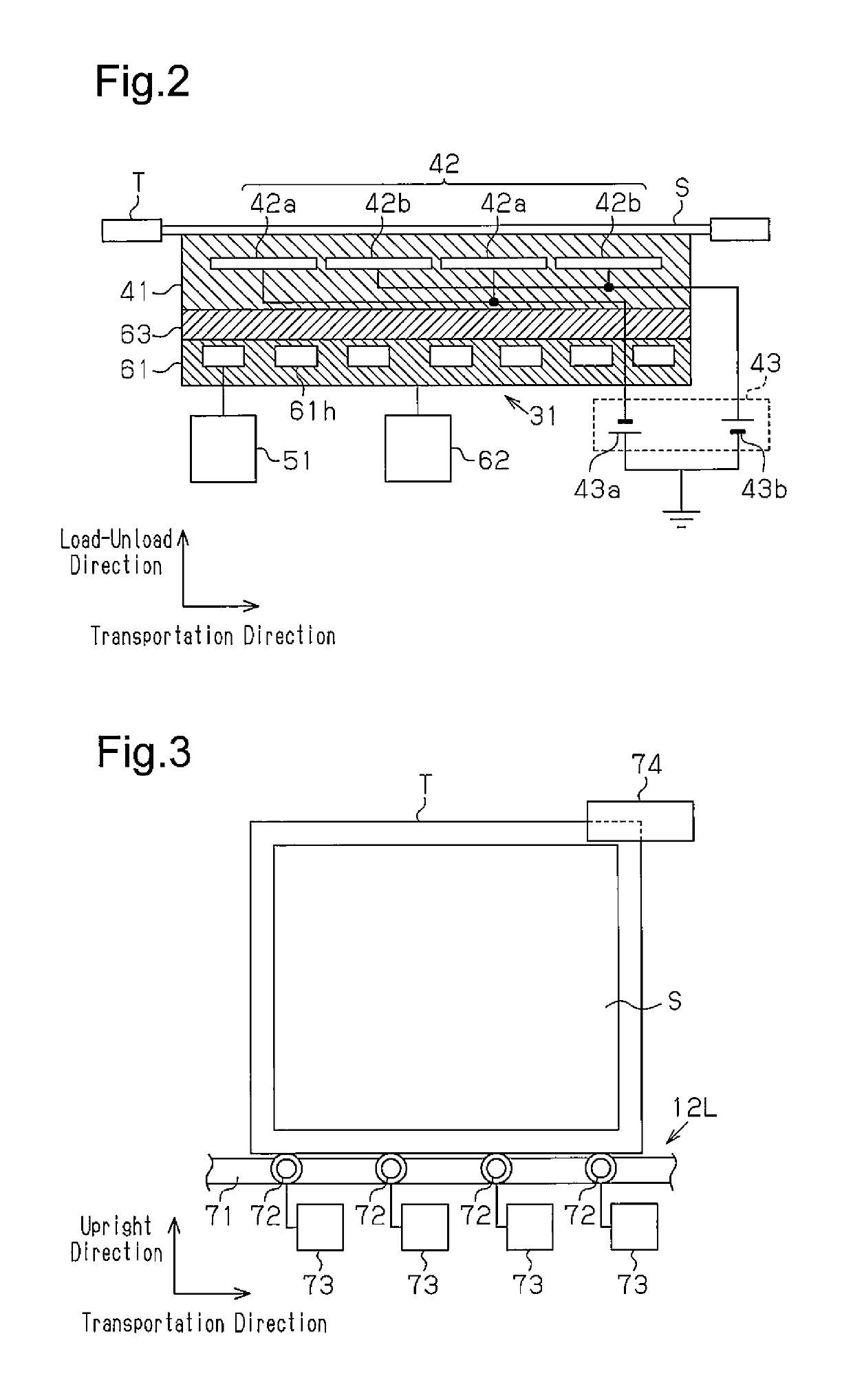
[0050]A thin substrate processing device according to a first embodiment will now be described with reference to FIG. 1 to FIG. 12. In the present embodiment, the thin substrate processing device is a sputtering device, for example.

[0051][Entire Configuration of Sputtering Device]

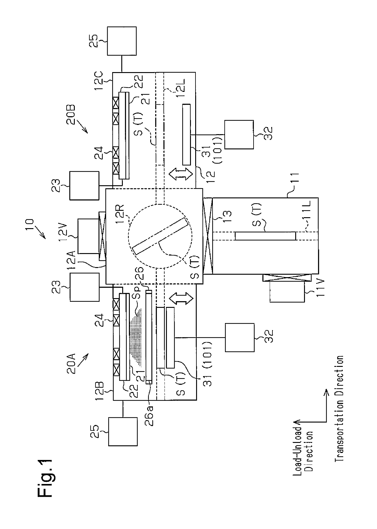
[0052]The entire configuration of a sputtering device 10 will now be described with reference to FIG. 1. As shown in FIG. 1, the sputtering device 10 includes a load-unload chamber 11 and a vacuum chamber 12. The load-unload chamber 11 and the vacuum chamber 12 are formed in box shapes, for example. Between the load-unload chamber 11 and the vacuum chamber 12, a gate valve 13 connects or disconnects the load-unload chamber 11 and the vacuum chamber 12. The load-unload chamber 11 loads and unloads a film substrate S as an example of a thin substrate along a load-unload direction shown in FIG. 1. The vacuum chamber 12 transports the film substrate S along a transportation direction shown in FIG. 1. The load-u...

example 1

[0119]After preparing a printed circuit board and a film substrate made of polyester resin, when forming a copper film on the printed circuit board and the film substrate, the voltage supplied to the chuck electrode of the electrostatic chuck was changed between the printed circuit board and the film substrate. Then, temperatures of the printed circuit board and the film substrate when forming the copper film at each voltage were measured. FIG. 10 shows the measurement result. In FIG. 10, the vertical axis shows a substrate temperature, and the horizontal axis shows the voltage (an absolute value) applied to the chuck electrode.

[0120]The printed circuit board was a substrate obtained by stacking a copper film and a glass epoxy resin layer on a glass epoxy substrate obtained by forming a copper foil on both surfaces of a film obtained by fixing a glass cloth (a core material) with the epoxy resin. A thickness of the printed circuit board was 80 μm, and a thickness of the film substra...

example 2

[0129]After reverse sputtering was performed on the surface of the insulation substrate made of glass epoxy resin, reverse sputtering speeds were measured at different positions with an effective range of the reverse sputtering of the insulation substrate. The size of the effective range of the reverse sputtering was 500 mm×600 mm, and the reverse sputtering was performed under the following condition. Reverse sputtering speeds were measured at two corners (first corner and second corner) located on a diagonal line in the effective range of the reverse sputtering, a central portion, and between each corner and the central portion. FIG. 11 shows the measurement result.

[0130]substrate: glass epoxy resin substrate

[0131]sputtering gas: argon gas

[0132]flow rate: 200 sccm

[0133]frequency: 2 MHz

[0134]electric power amount: 730 W

[0135]pressure: 2 Pa

[0136]As shown in FIG. 11, the reverse sputtering speed at the central portion of the effective range of the reverse sputtering was 1.9 nm / min, a...


PUM

PropertyMeasurementUnit
frequencyaaaaaaaaaa
frequencyaaaaaaaaaa
frequencyaaaaaaaaaa

Abstract

A thin substrate processing device include a substrate processing unit configured to process a thin substrate, and a cooling unit configured to cool the thin substrate when the substrate processing unit is processing the thin substrate.

Description

CLAIM OF PRIORITY[0001]This application is a U.S. National Stage Filing under 35 U.S.C. 371 from International Application No. PCT / JP2014 / 051856, filed on Jan. 28, 2014, and published as WO 2014 / 119580 A1 on Aug. 7, 2014, and claims the benefit of priority under 35 U.S.C. § 119 to Japanese Patent Application No. 2013-019768, filed on Feb. 4, 2013, and to Japanese Patent Application No. 2013-019767, filed on Feb. 4, 2013 which are hereby incorporated by reference herein in their entireties.TECHNICAL FIELD[0002]The technique of the present disclosure relates to a thin substrate processing device that processes a thin substrate such as a printed circuit board and a film substrate.BACKGROUND ART[0003]To mount electronic components onto a mounting substrate, the mounting substrate includes an adhesion layer, serving as an underlying layer for wires connected to the electronic components, and a seed layer, used to form the wires. To form each layer, plating or sputtering is performed (see...

Claims


Application Information

Patent Timeline
Patent Type & Authority Patents(United States)
IPC IPC(8): H01J37/34H01L21/67C23C14/50C23C14/54H01L21/683H01J37/32C23C14/34C23C14/56
CPCC23C14/541C23C14/345C23C14/50C23C14/568H01J37/32009H01J37/3244H01L21/6838H01J37/32715H01J37/32724H01J37/34H01J37/3464H01J37/3497H01L21/67109H01J37/32697
Inventor FUJINAGA, TETSUSHIMATSUMOTO, MASAHIROARAI, MAKOTOMASE, ERIKOIWAI, HARUNORITAKAHASHI, KOJIIHORI, ATSUHITO
Owner ULVAC INC
Why Eureka
Try Eureka