Fuse structure with thermal and crack-stop protection

a technology of fuse structure and thermal crackstop protection, which is applied in the direction of semiconductor devices, semiconductor/solid-state device details, electrical apparatus, etc., can solve the problems of term reliability, performance compromise, manufacturing yield compromis

Inactive Publication Date: 2002-08-22
GOOGLE LLC
View PDF0 Cites 39 Cited by
  • Summary
  • Abstract
  • Description
  • Claims
  • Application Information

AI Technical Summary

Problems solved by technology

However, increased density is generally accompanied by increased proximity of current-carrying structures which can compromise performance by increasing capacitance and capacitive coupling of such structures.
These materials often present additional problems of strength and / or thermal stability which may also compromise manufacturing yield and, hence, manufacturing economy, as well as some potential problems of long-term reliability.
However, this material will pass through a glass transition at roughly 450.degree. C., causing changes in stress.
This stress could cause damage in adjacent electrically active layers or cause delamination of the SiLK layer.
If any of these processes degrade the structure or allow cracks to develop in barrier layers, the chip may fail during use.
The SiLK layers are also poor barriers to oxygen diffusion, and if oxygen reaches metal conductor layers such as copper metallization, corrosion can result; compromising electrical integrity or at least increasing resistance (and propagation time) of the affected conductors.
Since SiLK is a relatively viscous film, cracks in the SiLK may or may not propagate, and such cracks are likely to terminate at the edge of a harder layer such as the nitride barriers.
Degradation is more likely to occur because of a catastrophic event at high temperature rather than a crack propagation event.
Therefore, while the silicide has a relatively low initial bulk resistance, although somewhat higher than metal, substantial heating and large temperature rise will be caused in the course of programming of a fuse.
Moreover, low-k dielectrics and SiLK in particular have very low thermal conductivity and can thus prevent or reduce heat transfer by which temperature rise can be limited.
Therefore, low-k organic materials proximate to a fuse will be sensitive to degradation during fuse programming.
Since a 1% yield failure is very significant, a 0.1% fuse reliability failure would be intolerable since such a rate would correspond to one or more instances on every chip where redundant circuits could not be substituted, if needed.
However, such a thickness is larger than desired for semiconductor processing when manufacturing tolerances are considered.
However, such placement is not generally consistent with thicker heat shields.
Evaluation of fuses created with such a silicide fuse show various sorts of degradation with occasional cracking of the hard dielectric adjacent to the fuse structure.
Such a crack must not be allowed to propagate to higher levels, particularly copper levels where electrical integrity is important.
However, no structure suitable for placement adjacent a fuse element that provides a location for termination of cracks has heretofore been known.

Method used


Image

  • Fuse structure with thermal and crack-stop protection
  • Fuse structure with thermal and crack-stop protection
  • Fuse structure with thermal and crack-stop protection

Examples


Embodiment Construction

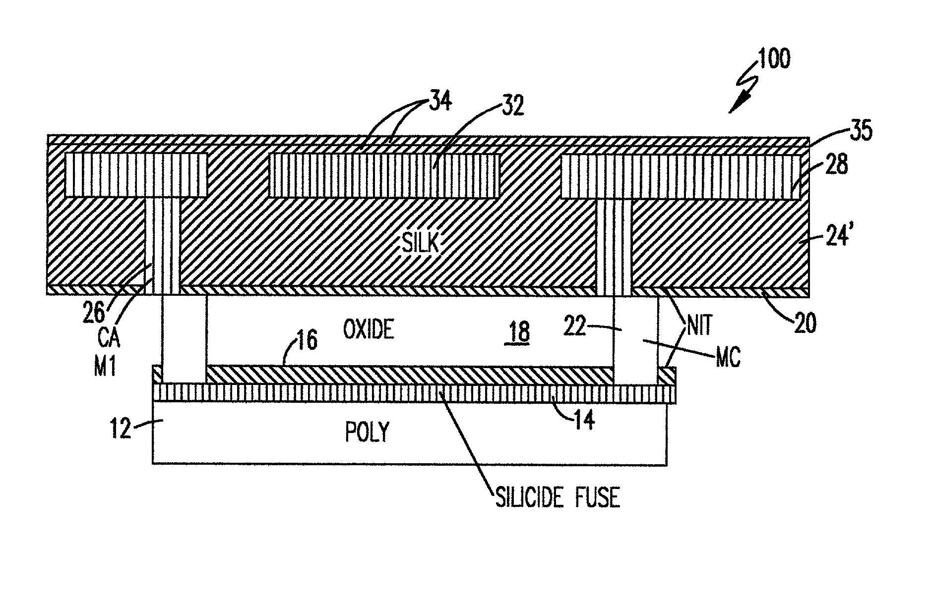
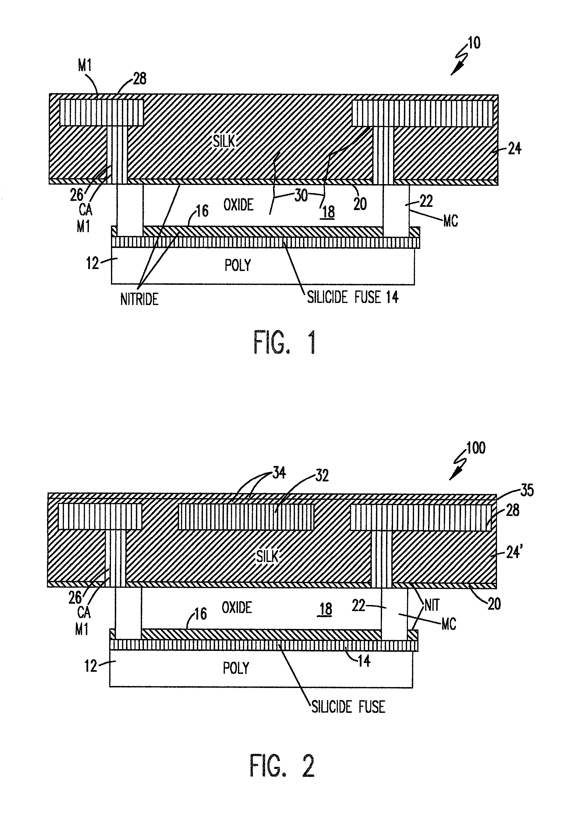
[0024] Referring now to the drawings, and more particularly to FIG. 1, there is shown, in cross-section, a fuse structure having a silicide fuse element exemplary of those in which cracking has been observed to occur. It is to be understood that while FIG. 1 does not include a structure in accordance with the invention, SiLK is shown as an exemplary low-k organic dielectric and thus is illustrative of how such a material would ordinarily be employed but for the problems noted above which are addressed by the present invention. Accordingly, no portion of FIG. 1 is admitted to be prior art with respect to the present invention. It should also be understood that the principles of the invention are applicable to other low-k organic dielectric materials other that SiLK; in regard to which the invention will be explained, below. SiLK, however, is the preferred environment and application of the invention in view of the particularly low dielectric constant, k, provided and the low temperat...


PUM

PropertyMeasurementUnit
temperatureaaaaaaaaaa
thickaaaaaaaaaa

Abstract

Thermal degradation of a low-k organic dielectric material is avoided or limited in the proximity of a heat source such as a fusible element by overlaying the low-k material with a thermally conductive material and providing a low thermal resistance path from the thermally conductive material, possibly having a low modulus of elasticity, to a heat sink. The thermally conductive material thus provides crack-stop protection for further layers of an integrated circuit or interconnect structure above the fusible element by mechanical, chemical and thermal encapsulation of the heat source and low-k material.

Description

[0001] 1. Field of the Invention[0002] The present invention generally relates to semiconductor integrated circuits and other connection arrangements which include fuses for programming thereof and, more particularly, to high density circuit structures utilizing low dielectric constant materials.[0003] 2. Description of the Prior Art[0004] It has long been recognized that increased density of circuit formation in integrated circuits and interconnect structures such as printed circuit boards yields potential increases in performance and functionality as well as manufacturing economy. However, increased density is generally accompanied by increased proximity of current-carrying structures which can compromise performance by increasing capacitance and capacitive coupling of such structures.[0005] Therefore, there has been substantial recent interest in insulators having particularly low dielectric constants for use between conductors in order to reduce capacitance and capacitive coupli...

Claims


Application Information

Patent Timeline
Patent Type & Authority Applications(United States)
IPC IPC(8): H01L23/373H01L23/525H01L23/532
CPCH01L23/3735H01L23/5256H01L23/5329H01L2924/0002H01L2924/00
Inventor ADKISSON, JAMES W.MACIEJEWSKI, EDWARDSMEYS, PETERSTAMPER, ANTHONY K.
Owner GOOGLE LLC
Why Eureka
Try Eureka