Multi-chip switch based on proximity communication

US20070291535A1Active Publication Date: 2007-12-20ORACLE INT CORP

Image

  • Multi-chip switch based on proximity communication
  • Multi-chip switch based on proximity communication
  • Multi-chip switch based on proximity communication

Examples


Embodiment Construction

[0042]The following description is presented to enable any person skilled in the art to make and use the invention, and is provided in the context of a particular application and its requirements. Various modifications to the disclosed embodiments will be readily apparent to those skilled in the art, and the general principles defined herein may be applied to other embodiments and applications without departing from the spirit and scope of the present invention. Thus, the present invention is not intended to be limited to the embodiments shown, but is to be accorded the widest scope consistent with the principles and features disclosed herein.

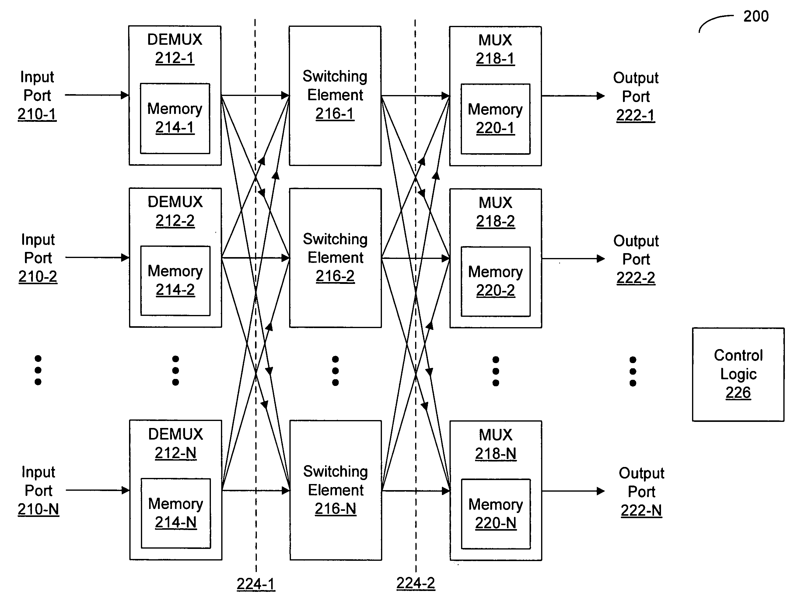
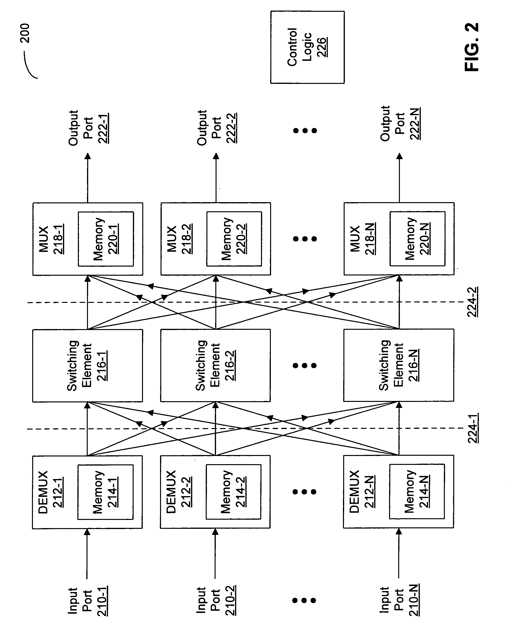
[0043]Embodiments of a method, a switch, and systems that include the switch are described. A semiconductor die in the switch communicates with other semiconductor dies and / or devices in the switch using proximity communication. In proximity communication, a first component (such as a semiconductor die or chip) is situated face-to-face with ano...


PUM


Abstract

A switch contains a first semiconductor die, which is configured to receive signals on a plurality of input ports and to output the signals on a plurality of output ports. The first semiconductor die is further configured to selectively couple the signals between the input and output ports using a plurality of switching elements in accordance with a set of control signals, which correspond to a configuration of the switch. During this process, a plurality of proximity connectors, proximate to a surface of the semiconductor die, are configured to communicate the signals by capacitive coupling.

Description

BACKGROUND[0001]1. Field of the Invention[0002]The present invention relates to techniques for communicating signals through switches. More specifically, the present invention relates to the design of a multi-chip switch comprised of semiconductor dies that communicate with each other using capacitively coupled proximity pads or connectors.[0003]2. Related Art[0004]Many computer systems and networks include switches to selectively communicate data items between different system components. These switches often include multiple input ports and multiple output ports, which are often implemented as high-speed serial input / output (I / O) ports. In contrast with lower-speed parallel ports, these high-speed serial ports offer advantages, such as a reduction in overall power consumption and in associated port area (in terms of the number of printed circuit boards, integrated circuit or chip packages, and / or I / O connectors). However, high-speed serial ports typically require additional circui...

Claims


Application Information

Patent Timeline
20 Dec 2007
Publication
US20070291535A1
IPC
G11C11/34
CPC
H04L49/109; H04L49/15; H04L49/3027; H04L49/254; H04L49/3018; H04L49/1515
Inventors
EBERLE, HANS; GURA, NILS