Apparatus and method for semiconductor bonding

a technology of apparatus and semiconductor, applied in the direction of electrical apparatus, semiconductor devices, basic electric elements, etc., can solve the problems of manufacturing losses, defects, and the cost of semiconductor devices in the production of consumer electrical and electronic devices, and achieve the effect of reducing conta

Active Publication Date: 2007-12-27
SUSS MICRO TEC LITHOGRAPHY
View PDF5 Cites 46 Cited by
  • Summary
  • Abstract
  • Description
  • Claims
  • Application Information

AI Technical Summary

Benefits of technology

[0006]Implementations of this aspect of the invention may include one or more of the following features. The force column comprises a plurality of forces arranged in a column having a base dimensioned to match the entire bond interface area between the first surfaces. The base's dimensions may be adjustable and may be adjusted to match bond interface areas having a diameter of 4 inches, 6 inches or 8 inches. The force column applies the pressure to the entire bond interface area with a uniformity of at least 90 percent. The pressure may be in the range of 1000 to 50000 mbars. The bond forming equipment includes an actuator configured to generate the force column. The actuator may be a solid plate driven by a pressurized gas or a pressurized fluid or a magnet. The positioning equipment comprises a clamp having a first clamp member configured to be brought in contact with a second surface of the first semiconductor structure and a second clamp member configured to be brought in contact with a second surface of the second semiconductor structure. The second surfaces of the first and second semiconductor structures are opposite to the first surfaces of the first and second semiconductor structures, respectively. Pressing the first and second semiconductor structures together with the force column comprises pressing at least one of the first and second clamp members with the force column. The apparatus may further include a frame configured to bear the load of the positioning and bond forming equipment. The frame may include at least one rigid post and the first and second clamp members are configured to be connected to the post so as to transfer any bending moments generated during the bonding of the semiconductor structures to the frame. Any or both of the first and second clamp members are movably connected to the rigid post. In one embodiment the frame comprises three rigid posts. The frame may further include top and bottom plates and the plates may be connected to the rigid posts. The apparatus may further include a controlled atmosphere chamber. The apparatus may further include a carrier fixture configured to transport the first and second semiconductor structures in and out of the chamber and to place the first and second semiconductor structures between the clamp members. The carrier fixture may include at least one spacer configured to maintain the first surfaces of the first and second semiconductor structures at a first distance. The carrier fixture may also have at least one clamp for clamping the first and second semiconductor structures together. The at least one spacer and the at least one clamp are independently actuated. The apparatus may further include a pin configured to stake the first surfaces of the first and second semiconductor structures before pressing the first and second semiconductor structures together with the force column. The pin stakes the first surfaces of the first and second semiconductor structures with an adjustable force. The chamber comprises a port dimensioned to allow transport of the carrier fixture in and out of the chamber. The apparatus may further include a pre-load chamber configured to communicate with the chamber via the port and the port may have a shutter for isolating the pre-load chamber from the chamber. The apparatus may also include a pressure gauge configured to monitor pressure in the chamber. The apparatus may further include equipment for aligning a first surface of the first clamp member parallel to a first surface of the second clamp member. The first surface of the first clamp member is configured to be brought in contact with the second surface of the first semiconductor structure and the first surface of the second clamp member is configured to be brought in contact with the second surface of the second semiconductor structure. The aligning equipment are configured to align the first and second semiconductor structures so that the force column is applied perpendicular to the bond interface area. The aligning equipment may include a linear alignment tool and a rotational alignment tool. The rotational aligning equipment is configured to rotationally align any of the first surfaces around a center of the bond interface area. The apparatus may further include equipment for heating the first and second semiconductor structures to reach a temperature uniformity of ±1 degree throughout the entire bond interface area. The apparatus may further include a thermal isolation system configured to thermally isolate the first and second semiconductor structures from the positioning and bond forming equipment. The thermal isolation system includes a vacuum isolation layer confined between an elastic membrane and a substrate comprising a low coefficient of thermal expansion (CTE) material. The low CTE substrate comprises a surface structured to minimize contact with the membrane. The heating equipment may include independently controlled multi-zone heaters configured to independently heat center and periphery regions of the first and second semiconductor structures. The heating equipment may include a first set of heaters configured to heat the first semiconductor substrate and a second set of heaters configured to heat the second semiconductor substrate and wherein the first set of heaters is arranged in a mirror image configuration of the second set of heaters. The semiconductor structures may be semiconductor wafers, flat panel structures, integrated circuit devices, 3D integrated microelectronics or Micro-Electro-Mechanical-Systems (MEMS). The first surfaces of the first and second semiconductor structures may further comprise first and second bond layers, respectively, and the first and second bond layers may be metal, semiconductor, insulator, adhesive, grid structures, glass, or insulators. The bonding may be anodic, eutectic, adhesive, fusion, glass frit or thermocompression bond.

Problems solved by technology

A major part of the cost in producing consumer electrical and electronic devices is the cost of the semiconductor devices that provide the very features that make the electronic devices so desired by consumers.
A significant factor in the determination of unit cost for semiconductor devices is defects that may present themselves in a given production lot.
As may be realized, loss of semiconductor devices through defects presents a fiscal loss to manufacturers that may generally be accommodated by increasing unit price.
However, although enabling the bond, the high forces also cause flex and distortion of conventional bonding tools that apply the forces, resulting in poor interfacial pressure uniformity, bond quality variability and wafer shift and defeating the improvements sought by using high bonding forces.

Method used


Image

  • Apparatus and method for semiconductor bonding
  • Apparatus and method for semiconductor bonding
  • Apparatus and method for semiconductor bonding

Examples


Embodiment Construction

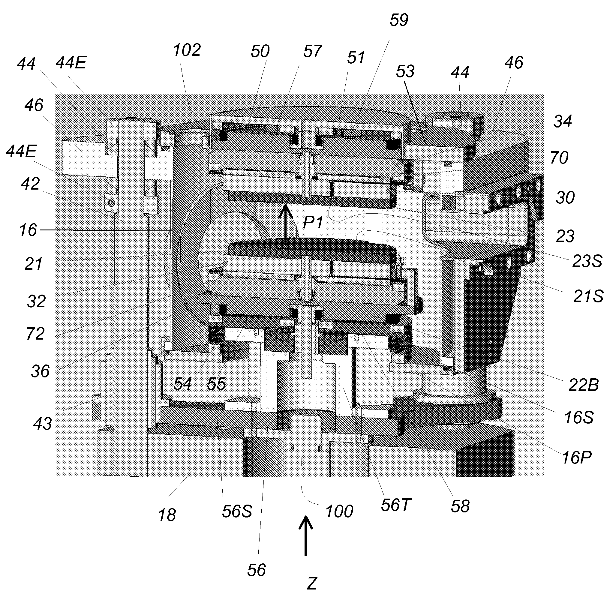
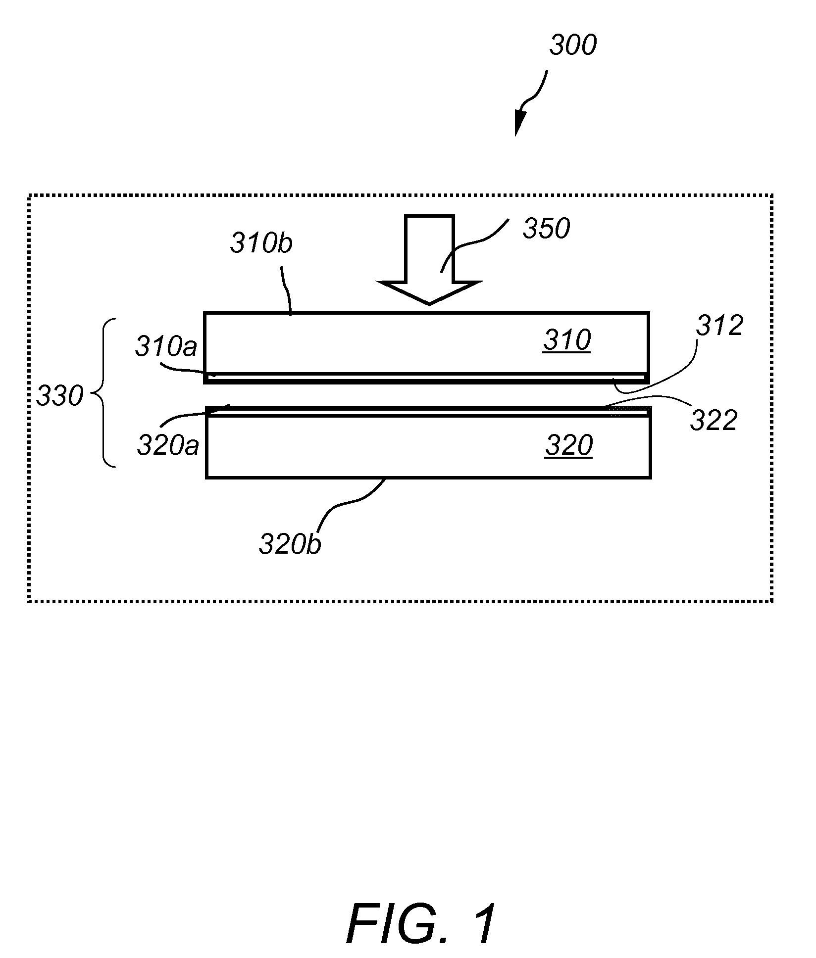
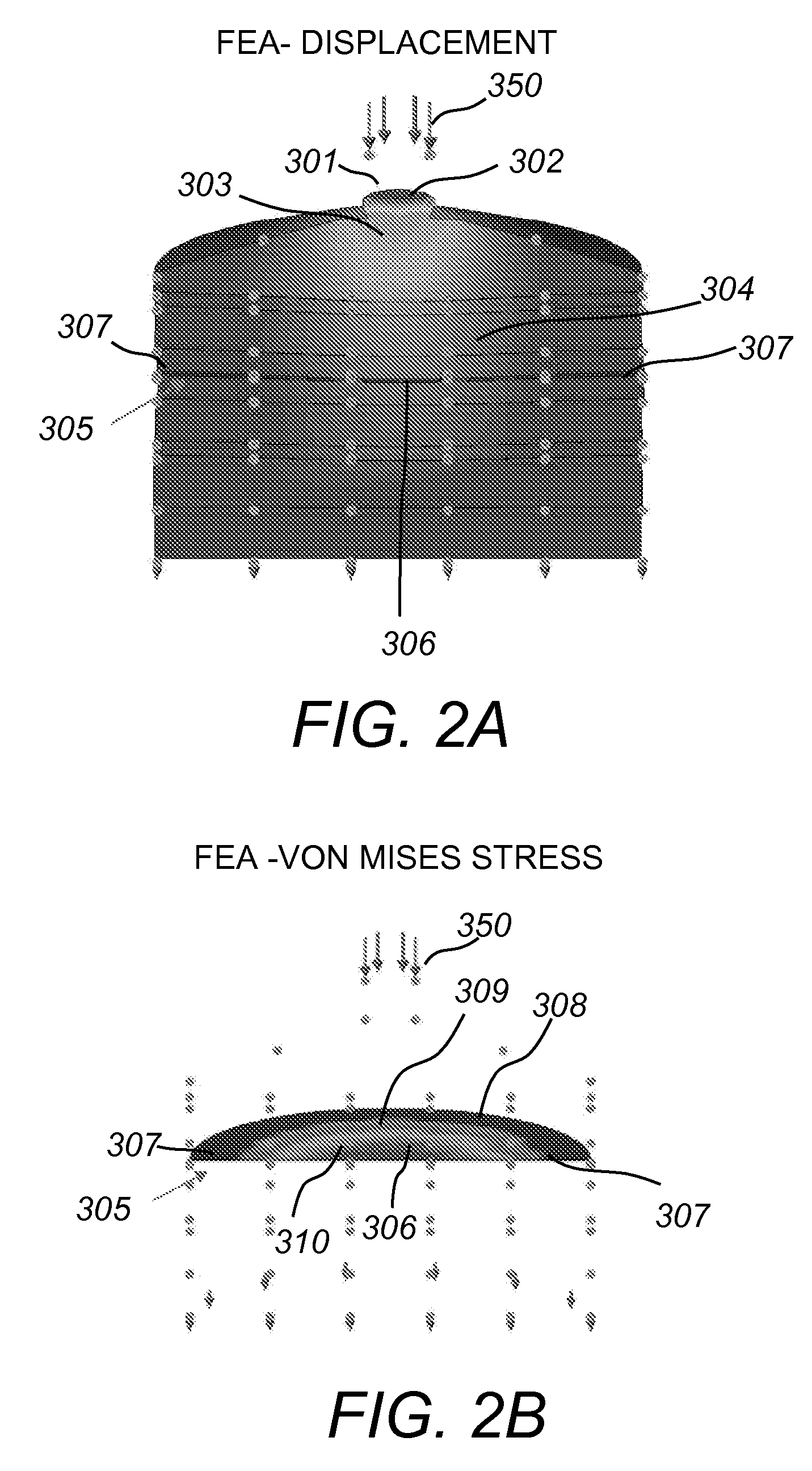
[0035]Referring to FIG. 1 in a prior art wafer bonding system 300 a first wafer 310 having a bond layer 312 on a first surface 310a is brought into contact with a second wafer 320 having a bond layer 322 on a first surface 320a, so that the two bond layers 312 and 322 are opposite to each other. The wafer bonding process involves compressing the two wafers together by applying a force 350 on a second surface 310b of the first wafer 310. Force 350 is usually applied to the center of the wafer stack 302 with a piston-type mechanism, as shown in FIG. 1. In other embodiments force 350 may be applied in the periphery of the wafer stack 302 or a second force may be applied simultaneously with the force 350 on the second surface 320b of the second wafer 320. Finite element analysis (FEA) of the displacement along the bond interface 305 is shown in FIG. 2A. We observe the formation of a “hot pressure spot” directly underneath the central area 301 where the force 350 is applied. A first sphe...


PUM


Abstract

An apparatus for bonding semiconductor structures includes equipment for positioning a first surface of a first semiconductor structure directly opposite and in contact with a first surface of a second semiconductor structure and equipment for forming a bond interface area between the first surfaces of the first and second semiconductor structures by pressing the first and second semiconductor structures together with a force column configured to apply uniform pressure to the entire bond interface area between the first surfaces.

Description

CROSS REFERENCE TO RELATED CO-PENDING APPLICATIONS[0001]This application claims the benefit of U.S. provisional application Ser. No. 60 / 815,619 filed Jun. 22, 2006 and entitled “HIGH-FORCE BOND TOOL”, the contents of which are expressly incorporated herein by reference.FIELD OF THE INVENTION[0002]The present invention relates to an apparatus and a method for semiconductor bonding, and more particularly to a high force semiconductor bonding apparatus and method.BACKGROUND OF THE INVENTION[0003]Consumers desire ever cheaper electrical and electronic devices. A major part of the cost in producing consumer electrical and electronic devices is the cost of the semiconductor devices that provide the very features that make the electronic devices so desired by consumers. Manufacturers of the semiconductor devices thus continue to seek ways to lessen manufacturing costs of the semiconductors. A significant factor in the determination of unit cost for semiconductor devices is defects that may...

Claims


Application Information

Patent Timeline
Patent Type & Authority Applications(United States)
IPC IPC(8): H01L27/12
CPCH01L21/67092H01L21/187H01L21/50H01L21/683
Inventor GEORGE, GREGORYHANCOCK, ETIENNECAMPBELL, ROBERT
Owner SUSS MICRO TEC LITHOGRAPHY
Why Eureka
Try Eureka