Semiconductor device having symbol pattern utilized as indentification sign and its manufacture method

a technology of indentification sign and semiconductor device, which is applied in the direction of semiconductor device, semiconductor/solid-state device details, electrical apparatus, etc., to achieve the effect of suppressing the generation of adverse effects

Active Publication Date: 2007-12-27
FUJITSU LTD
View PDF2 Cites 16 Cited by
  • Summary
  • Abstract
  • Description
  • Claims
  • Application Information

AI Technical Summary

Benefits of technology

[0028]The size of a symbol pattern is set to satisfy the above-described condition so that the symbol pattern can be formed at generally the same precision as that of the device pattern. It is therefore possible to suppress the generation of adverse effects to be caused by a defective shape of the symbol pattern.

Problems solved by technology

Various problems therefore occur if the size and shape of a symbol pattern to be formed at the same time when a device pattern is formed are greatly different from the size and shape of the device pattern.

Method used


Image

  • Semiconductor device having symbol pattern utilized as indentification sign and its manufacture method
  • Semiconductor device having symbol pattern utilized as indentification sign and its manufacture method
  • Semiconductor device having symbol pattern utilized as indentification sign and its manufacture method

Examples


Embodiment Construction

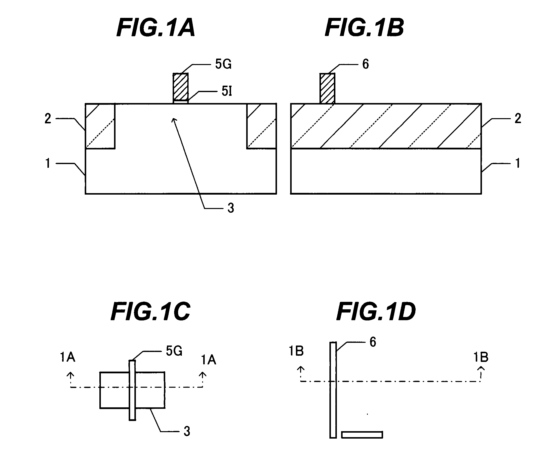
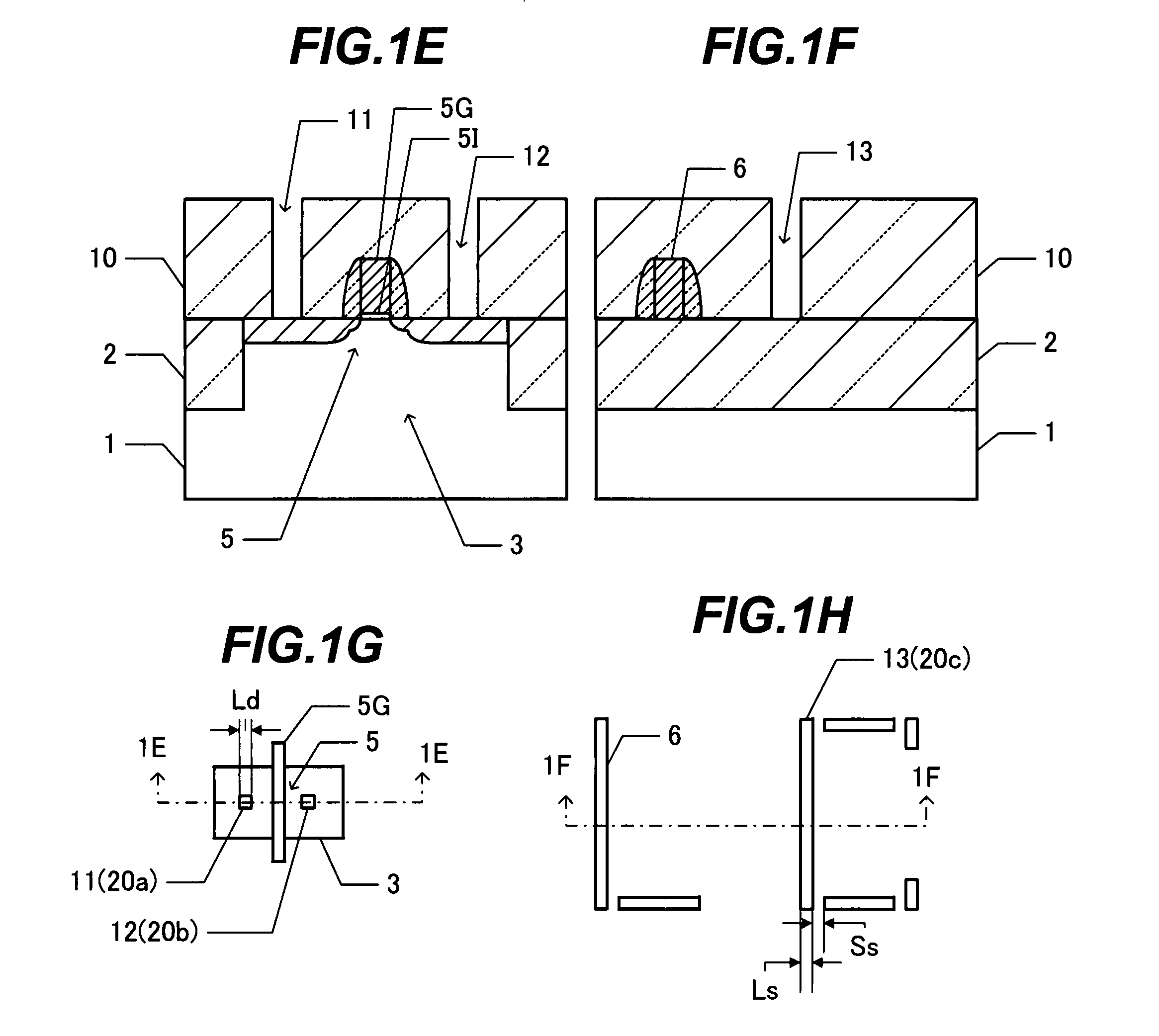
[0041]With reference to FIGS. 1A to 1N, description will be made on a semiconductor device manufacture method according to an embodiment.

[0042]FIGS. 1A and 1B are cross sectional views respectively showing regions of a substrate where a device pattern and a symbol pattern are disposed. FIGS. 1C and 1D are plan views of the regions shown in FIGS. 1A and 1B, respectively. FIGS. 1A and 1B are cross sectional views taken along one-dot chain lines 1A-IA and 1B-1B shown in FIGS. 1C and 1D, respectively.

[0043]An isolation insulating film 2 is formed in a surface layer of a semiconductor substrate 1 of silicon to define active regions 3. For example, the isolation insulating film 2 is formed by a shallow trench isolation (STI) method. A gate electrode 5G of polysilicon or the like is formed on a partial surface of the active region 3, intersecting with the active region 3. A gate insulating film 5I of silicon oxide or the like is disposed between the gate electrode 5G and semiconductor subs...


PUM


Abstract

A plurality of device patterns constituting part of an electronic circuit are formed over the surface of a substrate. A symbol pattern to be used for an identification sign is formed in the same layer as the device patterns. A width of the device pattern is within a pattern width range on a design rule. The symbol pattern is formed by a plurality of isolated element patterns. The element pattern is either a linear pattern or a dot pattern. A width of the element pattern is equal to or larger than 0.8 time a lower limit value of the pattern width range and equal to or smaller than 1.2 times an upper limit value of the pattern width range.

Description

CROSS REFERENCE TO RELATED APPLICATION[0001]This application is based on and claims priority of Japanese Patent Application No. 2006-172253 filed on Jun. 22, 2006, the entire contents of which are incorporated herein by reference.BACKGROUND OF THE INVENTION[0002]A) Field of the Invention[0003]The present invention relates to a semiconductor device having a symbol pattern utilized as an identification sign for wafers, chips, processes and the like, and its manufacture method.[0004]B) Description of the Related Art[0005]In the manufacture of semiconductor devices, symbol patterns such as characters are formed in a semiconductor chip or in a scribe line, at the same time when device patterns are formed in order for process control, product control or the like. This symbol pattern is observed with a microscope or the like during or after manufacture to be utilized as an identification sign for products and processes.[0006]JP-A-HEI-3-82051 discloses a semiconductor device manufacture met...

Claims


Application Information

Patent Timeline
Patent Type & Authority Applications(United States)
IPC IPC(8): H01L23/544H01L21/304
CPCH01L23/544H01L23/585H01L2223/54406H01L2223/54433H01L2223/5446H01L2924/0002H01L2223/5448H01L2924/00
Inventor YOSHIDA, SHIGEKIUSHIDA, FUMIONAORI, NOBUHISAOZAKI, YASUTAKA
Owner FUJITSU LTD
Why Eureka
Try Eureka