Semiconductor package, method of production of same, printed circuit board, and electronic apparatus

Inactive Publication Date: 2008-01-10
FUJITSU LTD
View PDF4 Cites 6 Cited by
  • Summary
  • Abstract
  • Description
  • Claims
  • Application Information

AI Technical Summary

Benefits of technology

[0011]Accordingly, in consideration with the above problems, an object of the present invention is to provide a semiconductor package reducing the influence due to thermal stress and therefore resistant to breakage and able to improve the reliability and a method of production of the same.
[0012]To attain the above object, the present invention provides a semiconductor package provided

Problems solved by technology

On the other hand, the higher density of circuit elements accompanying the smaller size and the faster speed of circuit operation accompanying the higher functions tend to result in remarkably increased generation of heat from the semiconductor chip.
There is therefore a limit to the heat radiation capability.
However, on the other hand, the semiconductor chip itself or the boundary portion between the semiconductor ch

Method used


Image

  • Semiconductor package, method of production of same, printed circuit board, and electronic apparatus
  • Semiconductor package, method of production of same, printed circuit board, and electronic apparatus
  • Semiconductor package, method of production of same, printed circuit board, and electronic apparatus

Examples


Embodiment Construction

[0024]Preferred embodiments of the present invention will be described in detail below while referring to the attached figures.

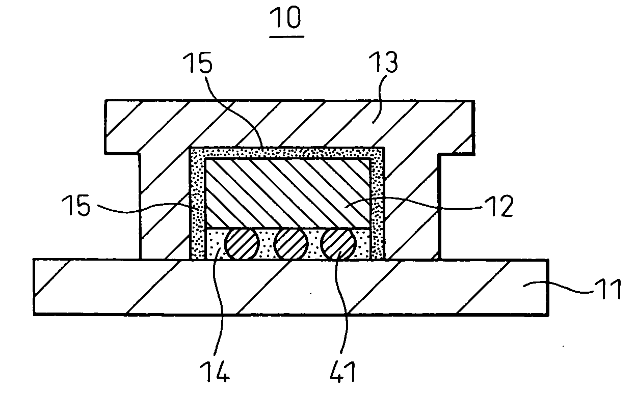
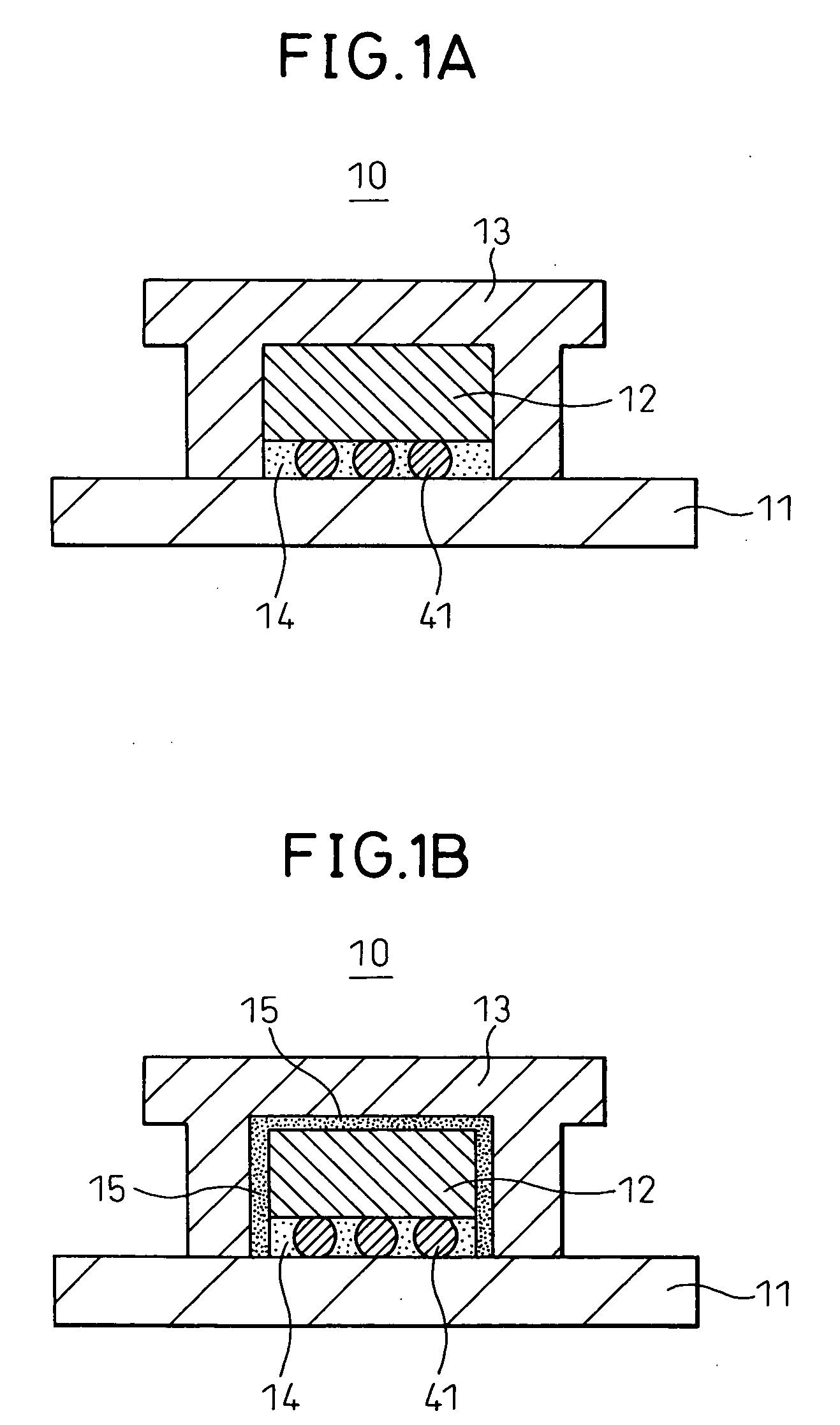
[0025]FIG. 1A and FIG. 1B are cross-sectional views showing first and second basic configurations according to the present invention.

[0026]Each of the semiconductor packages 10 according to the basic configurations shown in FIGS. 1A and 1B is a semiconductor package provided with a semiconductor chip 12, a board 11 supporting this semiconductor chip 12 at its bottom surface, and a heat radiator 13 provided on a back surface of this semiconductor chip 12. First, according to the basic configuration of FIG. 1A, a semiconductor package comprised of a semiconductor chip 12 enclosed fixed in place with its outer circumference in close contact with a board 11 and a heat radiator 13 is provided.

[0027]On the other hand, the semiconductor package 10 of FIG. 1B is comprised of a semiconductor chip 12 with resin filled at its bottom side (underfill 14) and a board 11 a...


PUM


Abstract

A semiconductor package provided with a heat radiator achieving a further improvement of reliability by reducing an influence of thermal stress. For this purpose, the heat radiator is formed by a heat radiator comprised of a heat radiation plate plus a box shaped part and comprised so that the entire semiconductor chip is enclosed in this box shaped part together with a board via a metallic bonding material.

Description

BACKGROUND OF THE INVENTION[0001]1. Field of the Invention[0002]The present invention relates to a semiconductor package, more particularly relates to a semiconductor package provided with an LSI or other semiconductor chip, a printed circuit board supporting this semiconductor chip at its bottom surface (hereinafter referred to as a “board”), and a heat spreader, heat sink, or other heat radiator provided on a back surface of the semiconductor chip. Further, it relates to a method of production of a semiconductor package, a printed circuit board, and an electronic apparatus.[0003]2. Description of the Related Art[0004]In recent years, to increase the density of mounting of semiconductor chips, mounting is changing to so-called flip chip mounting bonding a bare chip itself onto the board. This enables a further reduction of size and improvement of function of an information apparatus. On the other hand, the higher density of circuit elements accompanying the smaller size and the fas...

Claims


Application Information

Patent Timeline
IPC IPC(8): H01L23/495
CPCH01L21/563H01L23/3128H01L2224/73204H01L2224/32225H01L2224/16225H01L2924/19105H01L2924/16152H01L2924/16151H01L2924/15311H01L2924/01079H01L2224/83104H01L2224/73253H01L23/36H01L23/42H01L2224/73203H01L2924/00H01L2924/00011H01L2924/00014H01L2224/0401
Inventor NAKAMURA, NAOAKIYOSHIMURA, HIDEAKIFUKUZONO, KENJISATO, TOSHIHISA
Owner FUJITSU LTD
Why Eureka
Try Eureka