Light-emitting element, light-emitting device, and electronic device

a technology of light-emitting elements and electronic devices, which is applied in the direction of discharge tubes/lamp details, discharge tubes luminescnet screens, electric discharge lamps, etc., can solve the problems of short lifetime of light-emitting elements and poor durability of hole blocking layers, and achieve long lifetime, high luminous efficiency, and suppress the effect of time of carrier balan

Inactive Publication Date: 2008-01-10
SEMICON ENERGY LAB CO LTD
View PDF9 Cites 37 Cited by
  • Summary
  • Abstract
  • Description
  • Claims
  • Application Information

AI Technical Summary

Benefits of technology

[0014]As a result of diligent study, the present inventors have found that when a layer for controlling movement of carriers is provided, change with time of carrier balance can be suppressed. Thus, the present inventors have also found that a light-emitting element having long lifetime can be obtained.
[0034]In a light-emitting element of the present invention, a layer for controlling movement of carriers is provided, and change with time of carrier balance can be suppressed. Therefore, a light-emitting element having a long lifetime can be obtained. Further, the light-emitting element of the present invention is applied to a light-emitting device and an electronic device, whereby a light-emitting device and an electronic device each of which has high luminous efficiency and reduced power consumption can be obtained. In addition, a light-emitting device and an electronic device each of which has a long lifetime can be obtained.

Problems solved by technology

However, as disclosed in the Non-Patent Document, the hole blocking layer has poor durability, and the light emitting element has a short lifetime.

Method used


Image

  • Light-emitting element, light-emitting device, and electronic device
  • Light-emitting element, light-emitting device, and electronic device
  • Light-emitting element, light-emitting device, and electronic device

Examples


embodiment mode 1

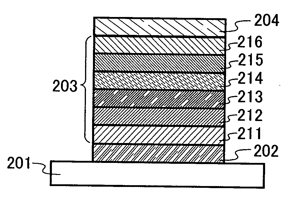
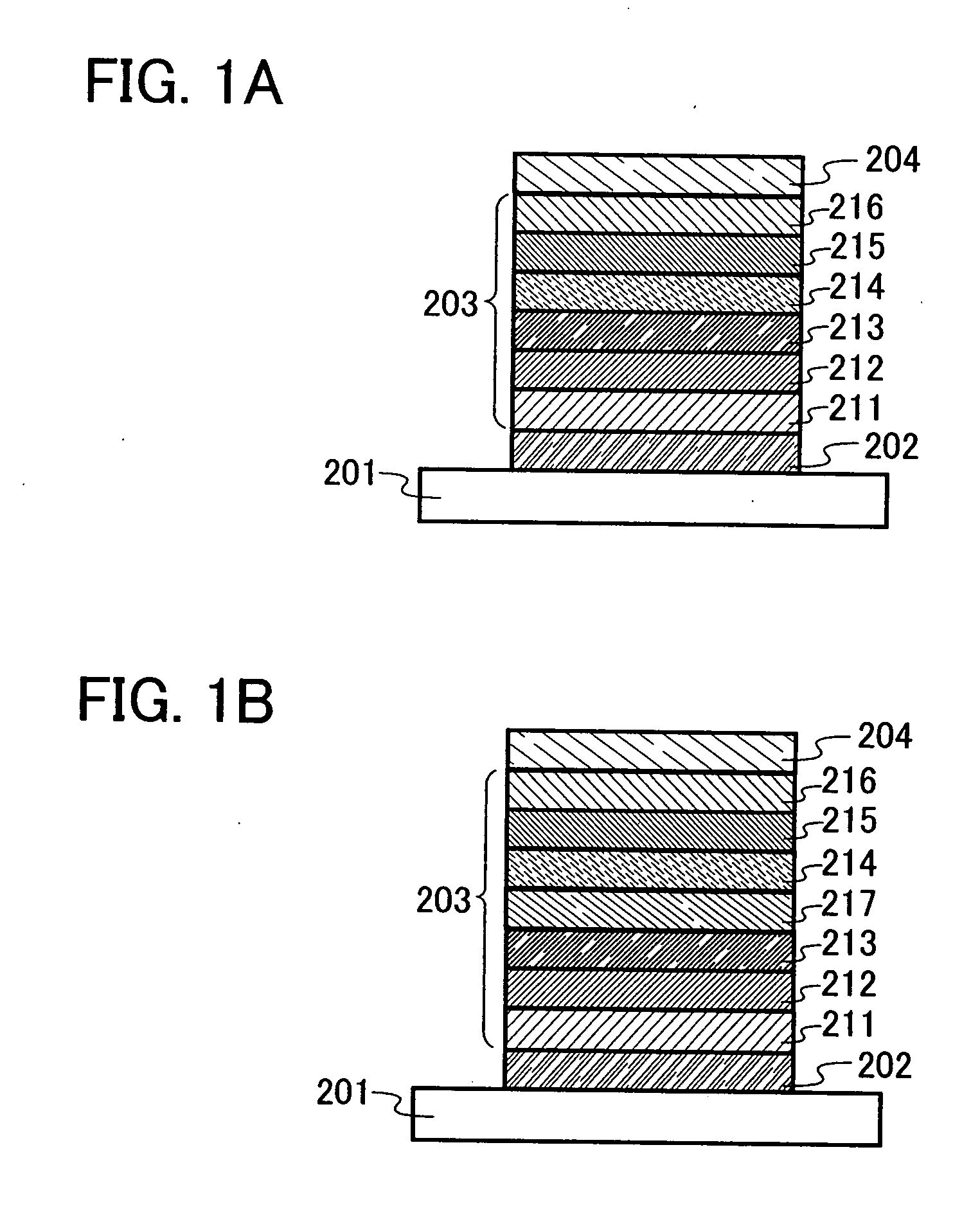
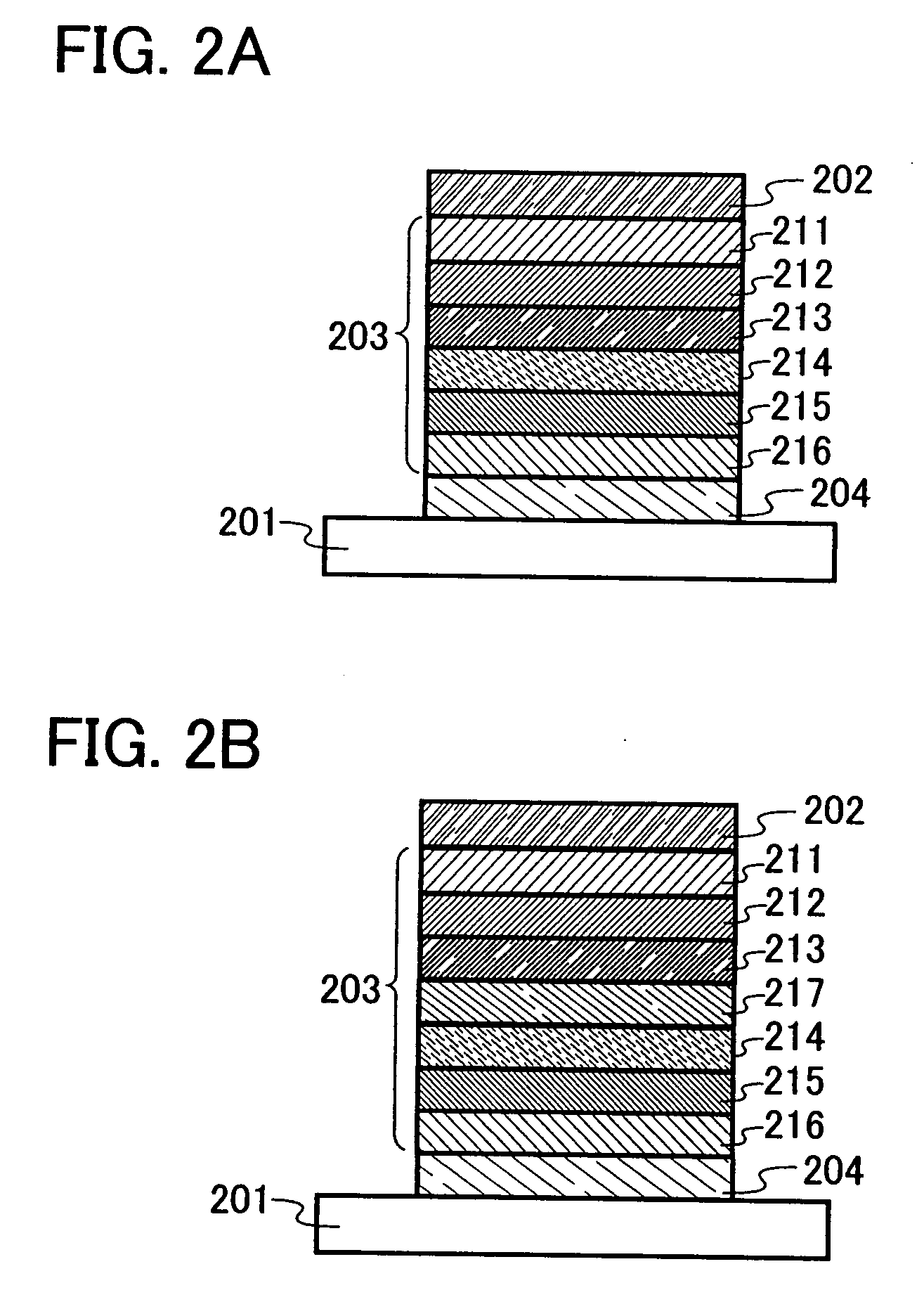
[0066]A mode of a light-emitting element of the present invention will be explained below with reference to FIG. 1A. In this embodiment mode, a light-emitting element provided with a layer for controlling movement of electrons as a layer for controlling movement of carriers will be explained. That is, in the present invention, carriers are recombined in a portion away from the electrodes using the layer for controlling movement of carriers in order to suppress change in carrier balance with time and to make a light-emitting element have a long lifetime.

[0067]In a light-emitting element of the present invention, a plurality of layers are provided between a pair of electrodes. The plurality of layers are stacked by combining layers including a substance having a high carrier injecting property or a substrate having a high carrier transporting property so that a light-emitting region is formed in a portion away from the electrodes, in other words, carriers are recombined in a portion a...

embodiment mode 2

[0135]In this embodiment mode, a mode of a light-emitting element, which is different from that of Embodiment Mode 1, of the present invention will be explained with reference to FIG. 5A. In this embodiment mode, a light-emitting element provided with a layer for controlling movement of holes as a layer for controlling movement of carriers will be explained. The light-emitting element of the present invention has a plurality of layers between a pair of electrodes. The plurality of layers are stacked by combining of layers including a substance having a high carrier injecting property and a substance having a high carrier transporting property so that a light-emitting region is formed in a portion away from the electrodes, in other words, carriers are recombined in a portion away from the electrodes.

[0136]In this embodiment mode, the light-emitting element includes a first electrode 402, a second electrode 404, and an EL layer 403 provided between the first electrode 402 and the seco...

embodiment mode 3

[0182]In this embodiment mode, a mode of a light-emitting element in which a plurality of light-emitting units of the present invention are stacked (hereinafter, this light-emitting element is referred to as a stacked-type element) will be explained with reference to FIG. 9. The light-emitting element is a stacked-type light-emitting element including a plurality of light-emitting units between a first electrode and a second electrode. Each of the light-emitting units may have a similar structure to that of the EL layer shown in Embodiment Mode 1 and Embodiment Mode 2. That is, the light-emitting elements shown in Embodiment Mode 1 and Embodiment Mode 2 are each a light-emitting element having one light-emitting unit, whereas the light-emitting element explained in this embodiment mode has a plurality of light-emitting units.

[0183]In FIG. 9, a first light-emitting unit 511 and a second light-emitting unit 512 are stacked between a first electrode 501 and a second electrode 502. The ...


PUM


Abstract

The light-emitting element of the present invention includes a light-emitting layer and a layer for controlling movement of carriers between a pair of electrodes. The layer for controlling movement of carriers includes a first organic compound having a carrier transporting property and a second organic compound for reducing the carrier transporting property of the first organic compound, and the second organic compound is dispersed in the first organic compound. The layer for controlling movement of carriers is provided in such a manner, whereby change in carrier balance with time can be suppressed. Therefore, a light-emitting element having a long lifetime can be obtained.

Description

BACKGROUND OF THE INVENTION[0001]1. Field of the Invention[0002]The present invention relates to light-emitting elements of a current excitation type. The present invention also relates to light-emitting devices and electronic devices each of which has the light-emitting device. More specifically, the invention relates to light-emitting elements of a current excitation type having a long lifetime. Further, the invention relates to light-emitting devices and electronic devices each of which uses the light-emitting device.[0003]2. Description of the Related Art[0004]In recent years, research and development have been extensively conducted on light-emitting elements using electroluminescence. As a basic structure of these light-emitting elements, a structure where a substance having light-emitting property is interposed between a pair of electrodes is used. By application of a voltage to this element, light emission from a substance having light-emitting property can be obtained.[0005]...

Claims


Application Information

Patent Timeline
Patent Type & Authority Applications(United States)
IPC IPC(8): H01J1/62
CPCH01L51/002H01L51/006H01L51/0062H01L51/0072H01L51/0073H01L51/504H01L51/5048H01L51/5052H01L51/5096H01L51/5016H01L51/0081H10K71/30H10K85/649H10K85/633H10K85/6574H10K85/324H10K85/6572H10K50/14H10K50/155H10K50/11H10K50/805H10K50/157H10K50/16H10K50/167H10K50/13H10K50/18H10K2101/10
Inventor SUZUKI, TSUNENORISEO, SATOSHINOMURA, RYOJI
Owner SEMICON ENERGY LAB CO LTD
Why Eureka
Try Eureka