Liquid crystal display device and electronic device

a technology of liquid crystal display and electronic device, which is applied in the direction of logic circuit coupling/interface arrangement, pulse technique, instruments, etc., can solve the problems of deterioration of the transistors formed of an amorphous semiconductor, and achieve the effects of low cost, high current supply capacity, and small siz

Active Publication Date: 2008-01-10
SEMICON ENERGY LAB CO LTD
View PDF18 Cites 159 Cited by
  • Summary
  • Abstract
  • Description
  • Claims
  • Application Information

AI Technical Summary

Benefits of technology

[0033]Note that in the invention, various types of transistors can be employed as a transistor without limiting to a certain type. Thus, for example, a thin film transistor (TFT) including a non-single crystalline semiconductor film typified by amorphous silicon or polycrystalline silicon can be employed. Accordingly, such a transistor can be formed at low temperature, can be formed at low cost, can be formed over a large substrate as well as a light-transmissive substrate, and further, such a transistor can transmit light. In addition, a transistor formed by using a semiconductor substrate or an SOI substrate, a MOS transistor, a junction transistor, a bipolar transistor, or the like can be employed. Accordingly, a transistor with few variations, a transistor with high current supply capacity, and a transistor with a small size can be formed, thereby a circuit with low power consumption can be formed by using such a transistor. In addition, a transistor including a compound semiconductor such as ZnO, a-InGaZnO, SiGe, or GaAs, or a thin film transistor obtained by thinning such a compound semiconductor can be employed. Therefore, such a transistor can be formed at low temperature, can be formed at room temperature, and can be formed directly over a low heat-resistant substrate such as a plastic substrate or a film substrate. A transistor or the like formed by an inkjet method or a printing method may also be employed. Accordingly, such a transistor can be formed at room temperature, can be formed at a low vacuum, or can be formed using a large substrate. In addition, since such a transistor can be formed without using a mask (a reticle), layout of the transistor can be easily changed. Further, a transistor including an organic semiconductor or a carbon nanotube, or other transistors can be employed. Accordingly, the transistor can be formed using a substrate which can be bent. Note that a non-single crystalline semiconductor film may include hydrogen or halogen. Moreover, a transistor can be formed using various types of substrates. The type of a substrate is not limited to a certain type. Therefore, for example, a single crystalline substrate, an SOI substrate, a glass substrate, a quartz substrate, a plastic substrate, a paper substrate, a cellophane substrate, a stone substrate, a stainless steel substrate, a substrate including a stainless steel foil, or the like can be used as a substrate. Furthermore, the transistor may be formed using one substrate, and then, the transistor may be transferred to another substrate. By using the aforementioned substrate, a transistor with excellent properties or a transistor with low power consumption can be formed, or a device with high durability or high heat resistance can be formed.
[0034]The structure of a transistor can be various modes without limiting to a certain structure. For example, a multi-gate structure having two or more gate electrodes may be used. When the multi-gate structure is used, a structure where a plurality of transistors are connected in series is provided because a structure where channel regions are connected in series is provided. By using the multi-gate structure, off-current can be reduced; the withstand voltage of the transistor can be increased to improve reliability; or a drain-sou...

Problems solved by technology

However, there has been a problem in that characteristics of transistors formed of ...

Method used


Image

  • Liquid crystal display device and electronic device
  • Liquid crystal display device and electronic device
  • Liquid crystal display device and electronic device

Examples


embodiment mode 1

[0138]In this embodiment mode, a basic principle of the invention is described with reference to

[0139]FIG. 1A.

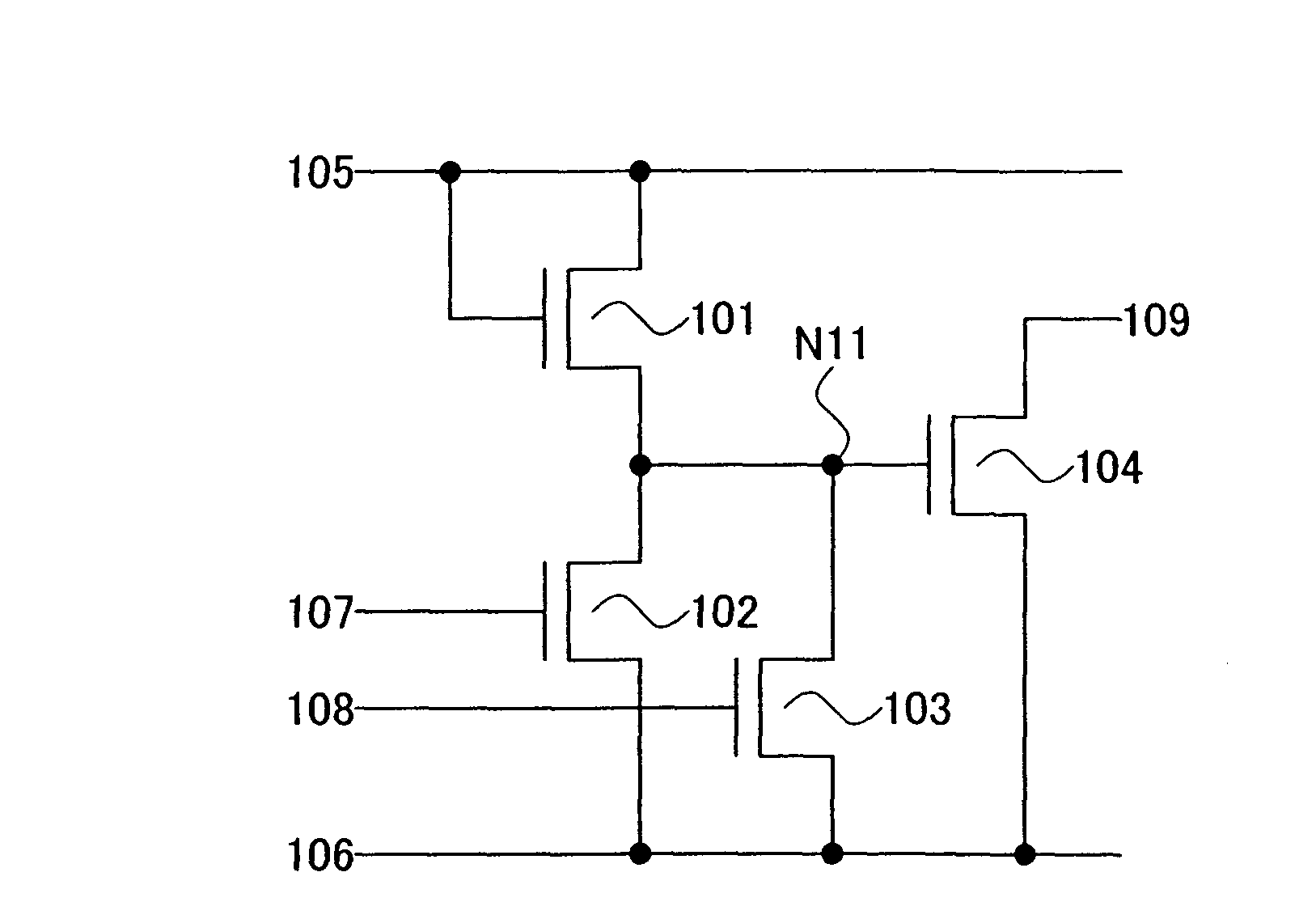
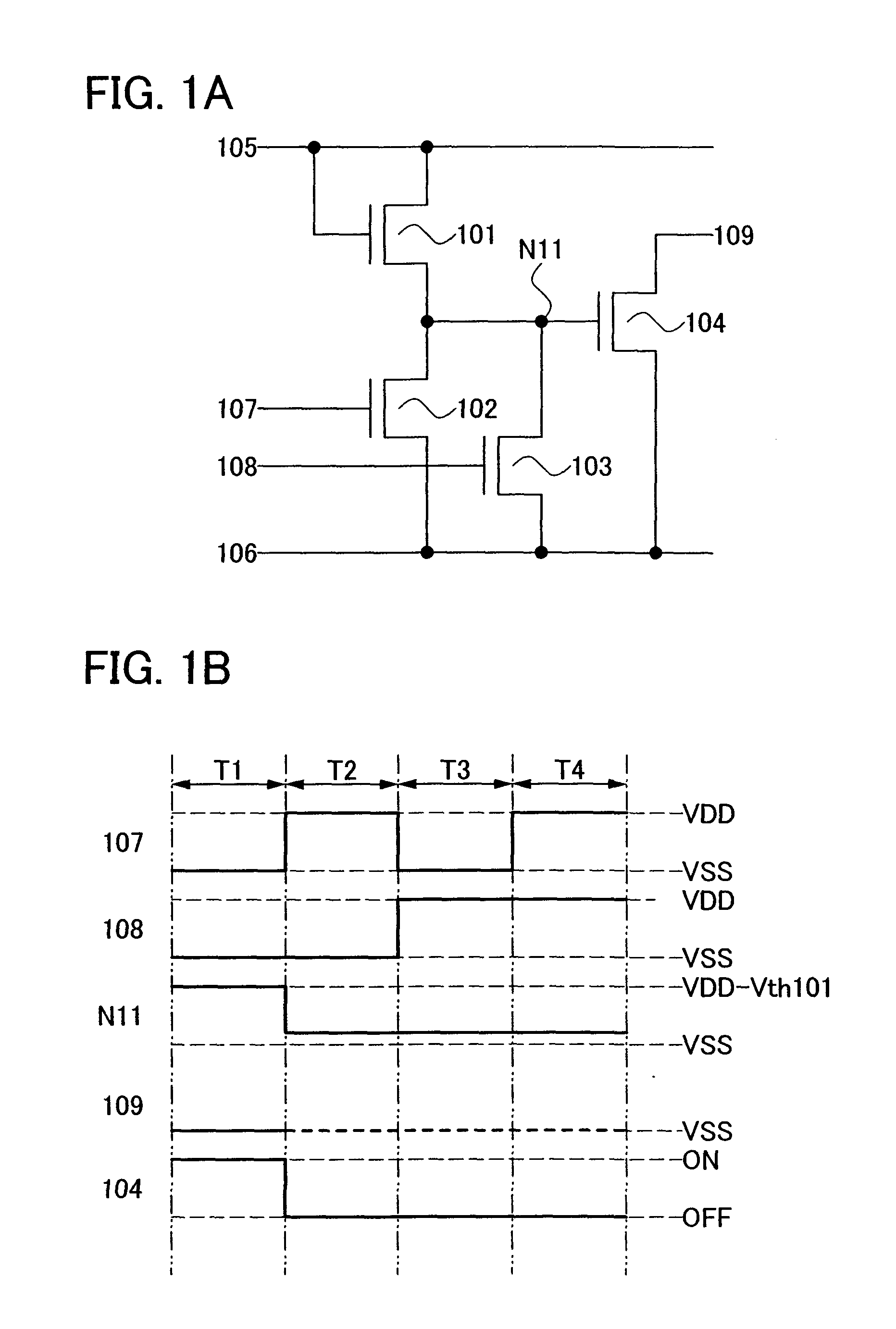
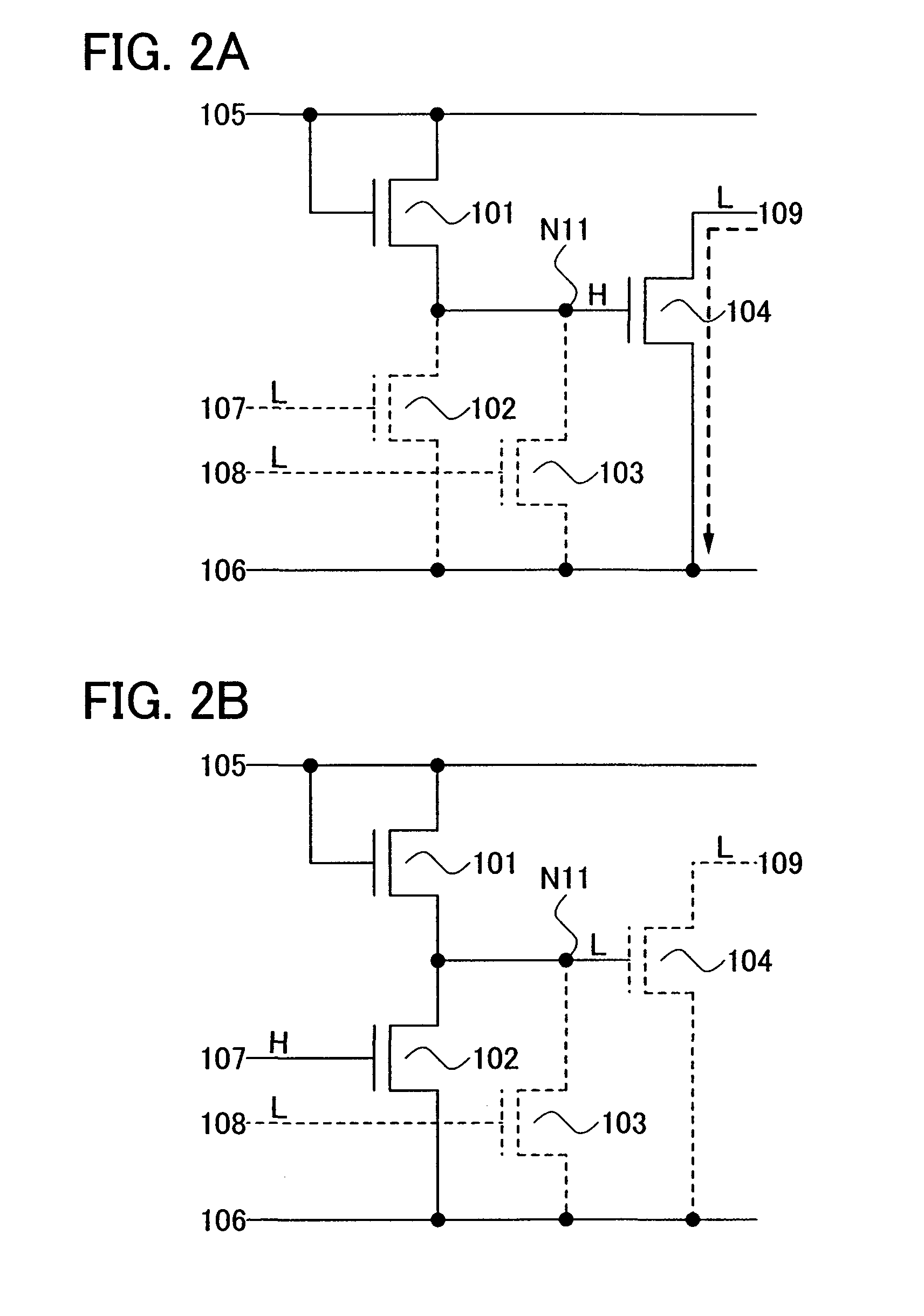
[0140]FIG. 1A shows a basic circuit which is based on the basic principle of the invention. The basic circuit in FIG. 1A includes a transistor 101, a transistor 102, a transistor 103, and a transistor 104.

[0141]Connection relations of the basic circuit in FIG. 1A are described. A gate of the transistor 101 is connected to a wiring 105, a first terminal of the transistor 101 is connected to the wiring 105, and a second terminal of the transistor 101 is connected to a gate of the transistor 104. A gate of the transistor 102 is connected to a wiring 107, a first terminal of the transistor 102 is connected to a wiring 106, and a second terminal of the transistor 102 is connected to the gate of the transistor 104. A gate of the transistor 103 is connected to a wiring 108, a first terminal of the transistor 103 is connected to the wiring 106, and a second terminal of the transisto...

embodiment mode 2

[0193]In this embodiment mode, a basic principle of the invention which is different from that of Embodiment Mode 1 is described with reference to FIG. 5A.

[0194]FIG. 5A shows a basic circuit which is based on the basic principle of the invention. The basic circuit in FIG. 5A includes a transistor 501, a transistor 502, a transistor 503, a transistor 504, a transistor 505, a transistor 506, and a transistor 507.

[0195]Connection relations of the basic circuit in FIG. 5A are described. A gate of the transistor 501 is connected to a wiring 508, a first terminal of the transistor 501 is connected to the wiring 508, and a second terminal of the transistor 501 is connected to a gate of the transistor 504. A gate of the transistor 502 is connected to a wiring 510, a first terminal of the transistor 502 is connected to a wiring 509, and a second terminal of the transistor 502 is connected to the gate of the transistor 504. A gate of the transistor 503 is connected to a wiring 511, a first te...

embodiment mode 3

[0255]In this embodiment mode, a basic principle of the invention which is different from those of Embodiment Modes 1 and 2 is described with reference to FIG. 9A.

[0256]FIG. 9A shows a basic circuit which is based on the basic principle of the invention. The basic circuit in FIG. 9A includes a transistor 901, a transistor 902, a transistor 903, and a transistor 904.

[0257]Connection relations of the basic circuit in FIG. 9A are described. A gate of the transistor 901 is connected to a gate of the transistor 904, a first terminal of the transistor 901 is connected to a wiring 906, and a second terminal of the transistor 901 is connected to the gate of the transistor 904. A gate of the transistor 902 is connected to a wiring 907, a first terminal of the transistor 902 is connected to a wiring 905, and a second terminal of the transistor 902 is connected to the gate of the transistor 904. A gate of the transistor 903 is connected to a wiring 908, a first terminal of the transistor 903 i...


PUM


Abstract

To provide a circuit used for a shift register or the like. The basic configuration includes first to fourth transistors and four wirings. The power supply potential VDD is supplied to the first wiring and the power supply potential VSS is supplied to the second wiring. A binary digital signal is supplied to each of the third wiring and the fourth wiring. An H level of the digital signal is equal to the power supply potential VDD, and an L level of the digital signal is equal to the power supply potential VSS. There are four combinations of the potentials of the third wiring and the fourth wiring. Each of the first transistor to the fourth transistor can be turned off by any combination of the potentials. That is, since there is no transistor that is constantly on, deterioration of the characteristics of the transistors can be suppressed.

Description

BACKGROUND OF THE INVENTION[0001]1. Field of the Invention[0002]The present invention relates to a semiconductor device. In addition, the invention relates to a display device having the semiconductor device. In particular, the invention relates to a liquid crystal display device having the semiconductor device and an electronic device having the liquid crystal display device.[0003]2. Description of the Related Art[0004]In recent years, with the increase of large display devices such as liquid crystal televisions, display devices such as liquid crystal display devices and light-emitting devices have been actively developed. In particular, a technique for forming a pixel circuit and a driver circuit including a shift register or the like (hereinafter referred to as an internal circuit) over the same substrate by using transistors made of an amorphous semiconductor over an insulator has been actively developed, because the technique greatly contributes to low power consumption and low...

Claims


Application Information

Patent Timeline
IPC IPC(8): H03K19/0175
CPCG09G3/20G09G2310/0267G09G2310/0286H01L21/84H01L27/12G02F1/1368G09G3/3677H01L27/156G02F1/13306G02F1/13624G02F1/136286G02F2001/136245H01L27/124H01L27/1222G02F1/136245H10K59/131H10K59/1213H01L27/1225G09G3/3648G09G2300/04G09G2300/08G09G2310/08H01L29/78696
Inventor UMEZAKI, ATSUSHI
Owner SEMICON ENERGY LAB CO LTD
Why Eureka
Try Eureka