Semiconductor memory device and control method of the same

Active Publication Date: 2008-01-24
KIOXIA CORP
View PDF3 Cites 133 Cited by
  • Summary
  • Abstract
  • Description
  • Claims
  • Application Information

AI Technical Summary

Benefits of technology

[0024]FIG. 14 is a view for explaining an advantageous effect of

Problems solved by technology

However, there is a limit to the erase voltage Vera that is to be applied and the number of pulses.
Consequently, if the characteristics have varied and the speed of the erase operation has decreased, the threshold voltages of the memory cells do not reach even if the erase voltage Vera reaches its uppe

Method used


Image

  • Semiconductor memory device and control method of the same
  • Semiconductor memory device and control method of the same
  • Semiconductor memory device and control method of the same

Examples


first embodiment

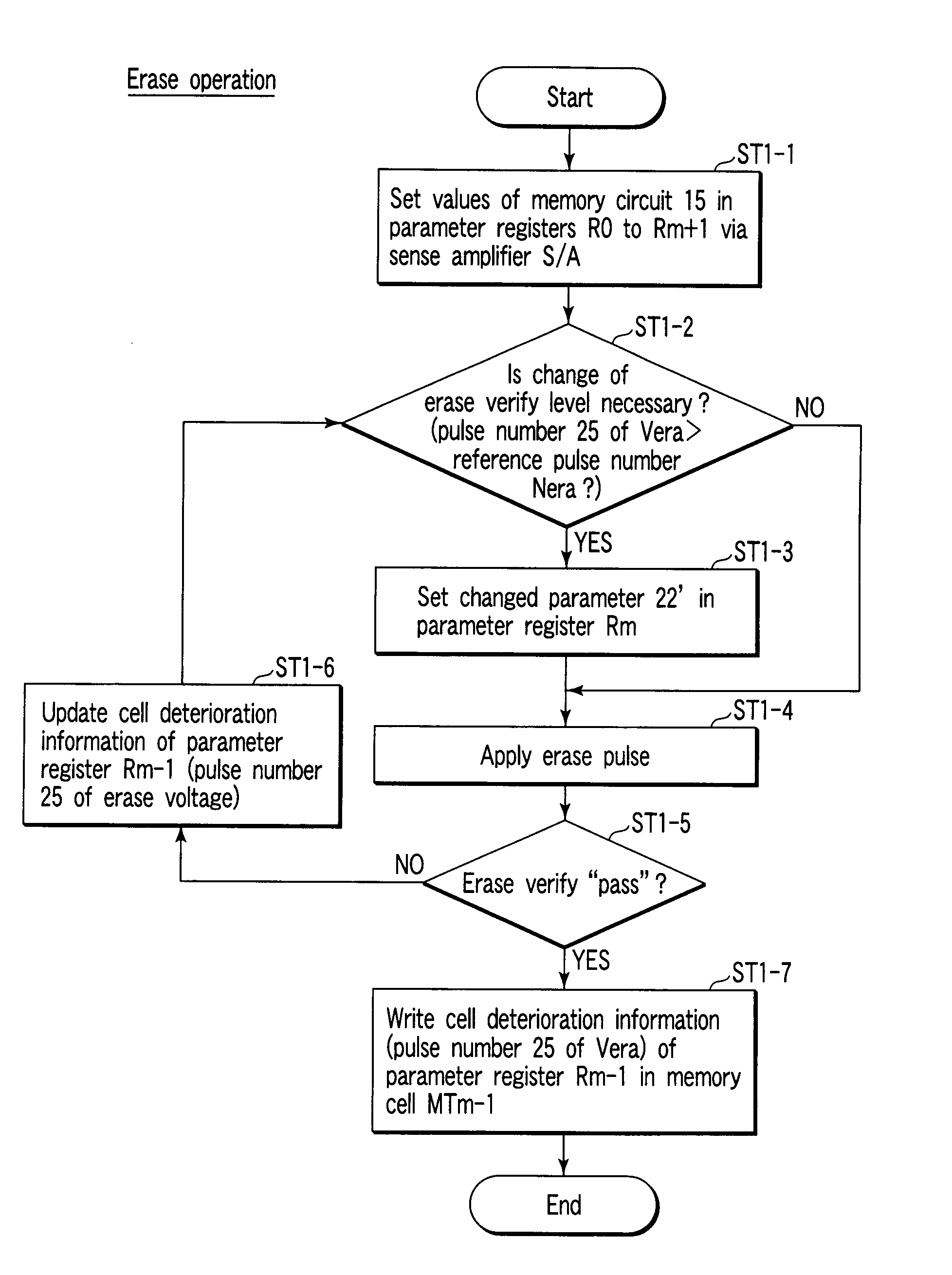
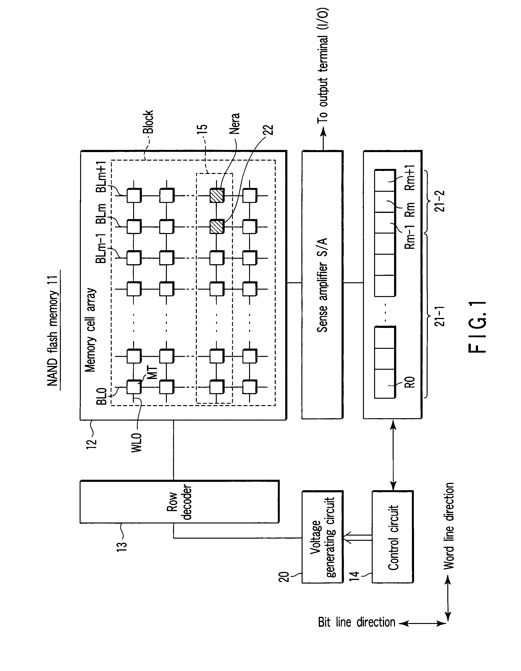
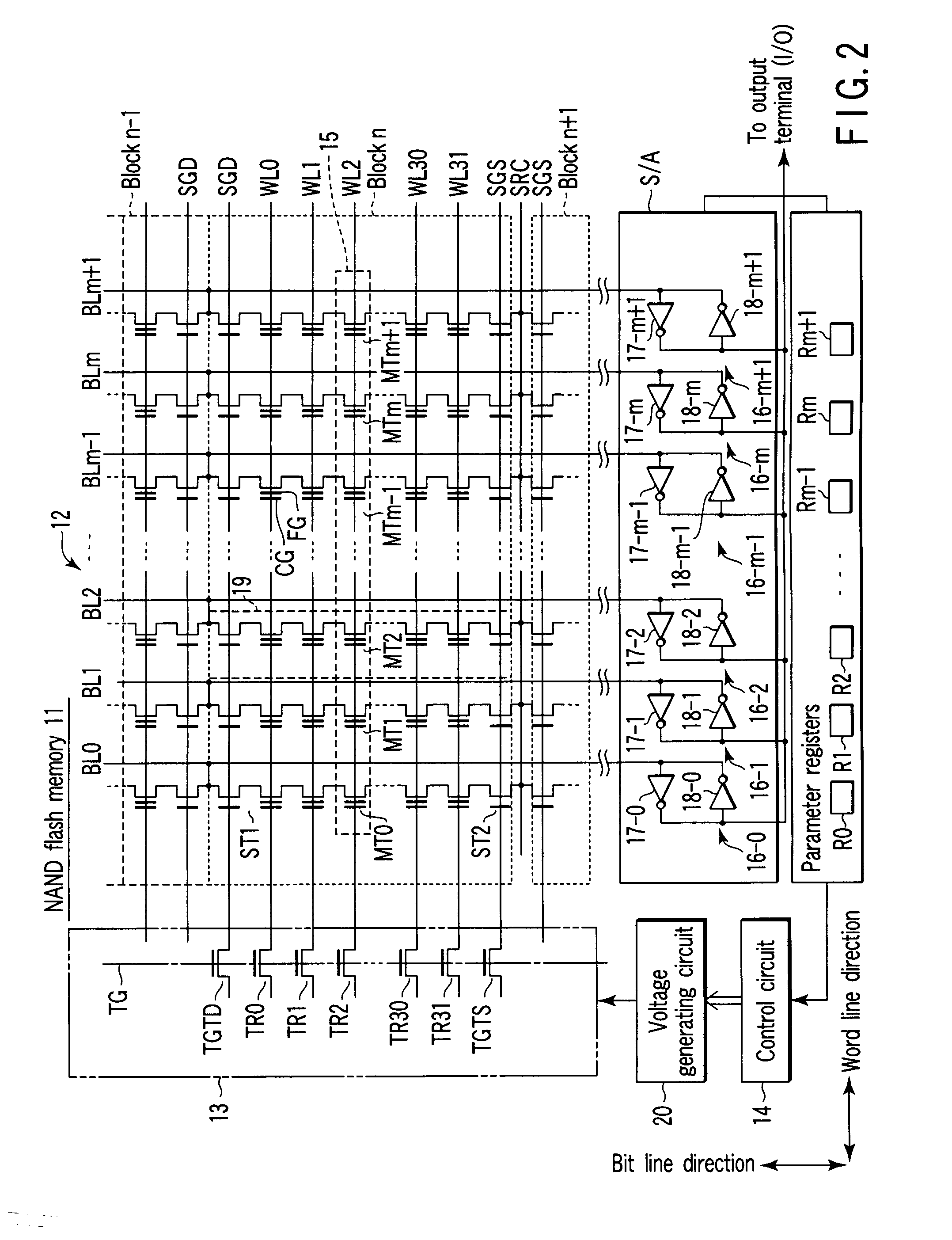
[0046] To begin with, referring to FIG. 1 and FIG. 2, a semiconductor memory device according to a first embodiment of the present invention is described. FIG. 1 is a block diagram showing the semiconductor memory device according to this embodiment, and FIG. 2 is a circuit diagram showing the semiconductor memory device according to the embodiment. In this embodiment, a NAND flash memory is described as an example of the semiconductor memory device.

[0047] As shown in FIG. 1 and FIG. 2, a NAND flash memory 11 includes a voltage generating circuit 20, a memory cell array 12, a row decoder 13, a sense amplifier S / A, a control circuit 14 and parameter registers R0 to Rm+1.

[0048] The voltage generating circuit 20 is configured to generate voltages of predetermined values, for example, a write voltage, an erase voltage and a read voltage.

[0049] The memory cell array 12 includes a plurality of Blocks (Block n−1, Block n, Block n+1, . . . ) and a memory circuit 15. In this example, the ...

second embodiment

Example Including a Cache Memory

[0116] Next, a semiconductor memory device according to a second embodiment of the invention is described with reference to FIG. 15. The second embodiment relates to an example in which a cache memory is further included. In the description below, a detailed description of the parts common to those in the first embodiment is omitted.

[0117] As shown in FIG. 15, the semiconductor memory device of the second embodiment differs from that of the first embodiment in that the semiconductor memory device further includes cache memories C0 to Cm+1 which have inputs connected to the sense amplifier S / A and have outputs connected to the parameter registers R0 to Rm+1. For example, an SRAM (Static Random-Access Memory) is applied to each of the cache memories C0 to Cm+1.

[0118] The parameter 22, etc. in the memory circuit 15 are read out batchwise in advance via the sense amplifier S / A into the cache memories C0 to Cm+1, for example, when power is turned on (po...

third embodiment

Example of Multilevel NAND Flash Memory

[0141] Next, referring to FIG. 20 to FIG. 30, a semiconductor memory device according to a third embodiment is described. This embodiment relates to an example in which the invention is applied to a multilevel NAND flash memory which is capable of storing multi-bit data in one memory cell. In the description below, a detailed description of the parts common to those in the first embodiment is omitted. In the present embodiment, a 4-value multilevel NAND flash memory is described as an example of the multilevel NAND flash memory.

[0142] To begin with, referring to FIG. 20, a description is given of an example of the structure of the semiconductor memory device according to the present embodiment.

[0143] As shown in FIG. 20, the semiconductor memory device of this embodiment differs from that of the first embodiment in the following respects.

[0144] The memory circuit 15 stores a reference pulse number NeraX, a voltage VsenX at a sense time (sen...


PUM


Abstract

A semiconductor memory device includes a memory cell array, a voltage generating circuit, a memory circuit which stores a reference pulse number of an erase voltage of the memory cell array and a parameter, and a control circuit which controls, when a pulse number of the erase voltage exceeds the reference pulse number of the erase voltage, the voltage generating circuit in a manner to increase at least an erase verify level in accordance with the parameter.

Description

CROSS-REFERENCE TO RELATED APPLICATIONS [0001] This application is based upon and claims the benefit of priority from prior Japanese Patent Applications No. 2006-198507, filed Jul. 20, 2006; and No. 2007-135717, filed May 22, 2007, the entire contents of both of which are incorporated herein by reference. BACKGROUND OF THE INVENTION [0002] 1. Field of the Invention [0003] The present invention relates to a semiconductor memory device and a control method of the semiconductor memory device, which are applied to, for instance, a NAND flash memory. [0004] 2. Description of the Related Art [0005] In recent years, a demand for nonvolatile memories has been increasing in accordance with an increase in memory capacity thereof. A NAND flash memory is an example of such nonvolatile memories (see, e.g. Jpn. Pat. Appln. KOKAI Publication No. 2004-14043). [0006] It is known, however, that in the memory cells of the NAND flash memory, if write / erase operations for data rewrite are repeated, the ...

Claims


Application Information

Patent Timeline
IPC IPC(8): G11C11/34
CPCG11C8/08G11C16/16G11C8/10
Inventor YANAGIDAIRA, KOSUKEFUKUDA, KOICHIHARA, TAKAHIKO
Owner KIOXIA CORP
Why Eureka
Try Eureka