Light emitting diode package with optical element

a technology of light-emitting diodes and optical elements, which is applied in the direction of basic electric elements, semiconductor devices, electrical apparatus, etc., can solve the problems of affecting the performance of the device, affecting the use of silicone,

Active Publication Date: 2008-01-31
CREELED INC
View PDF64 Cites 134 Cited by
  • Summary
  • Abstract
  • Description
  • Claims
  • Application Information

AI Technical Summary

Problems solved by technology

In addition, different colors of light are often generated from different types of LEDs which can require complex fabrication to combine in one device.
The resulting devices can also require complicated control electronics since the different diode types can require different control voltages.
Long term wavelength and stability of these devices is also degraded by the different aging behavior of the different LEDs.
Silicone lenses are typically molded using injection molding processes, which can place limitations on the properties of the silicone that may be used.
Glass lenses are typically formed using a melting process that can limit the possible geometries and add substantial piece part cost to the final lamp.
Typical wire bonded LEDs cannot be encapsulated in molten glass because of the high melting temperature of glass.
The parts also represent additional cost due to the required lens fabrication, and may be difficult to attach.
This can result in the cracking or delaminating of the LED chip or package elements, both of which can reduce light extraction from the LED package.
This difference in CTE can also result in damage to the LED chip, and in particular the wire bond can be broken or pulled from the LED resulting in failure of the LED package.

Method used


Image

  • Light emitting diode package with optical element
  • Light emitting diode package with optical element
  • Light emitting diode package with optical element

Examples


Embodiment Construction

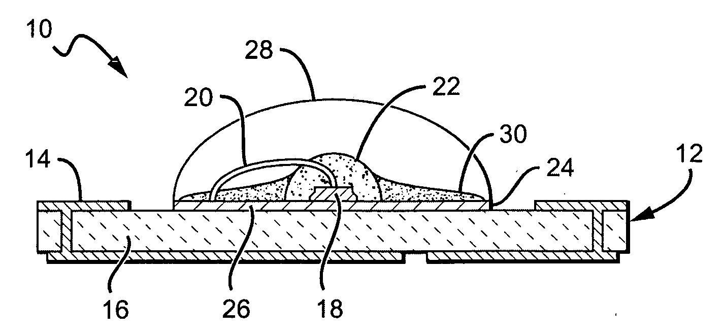
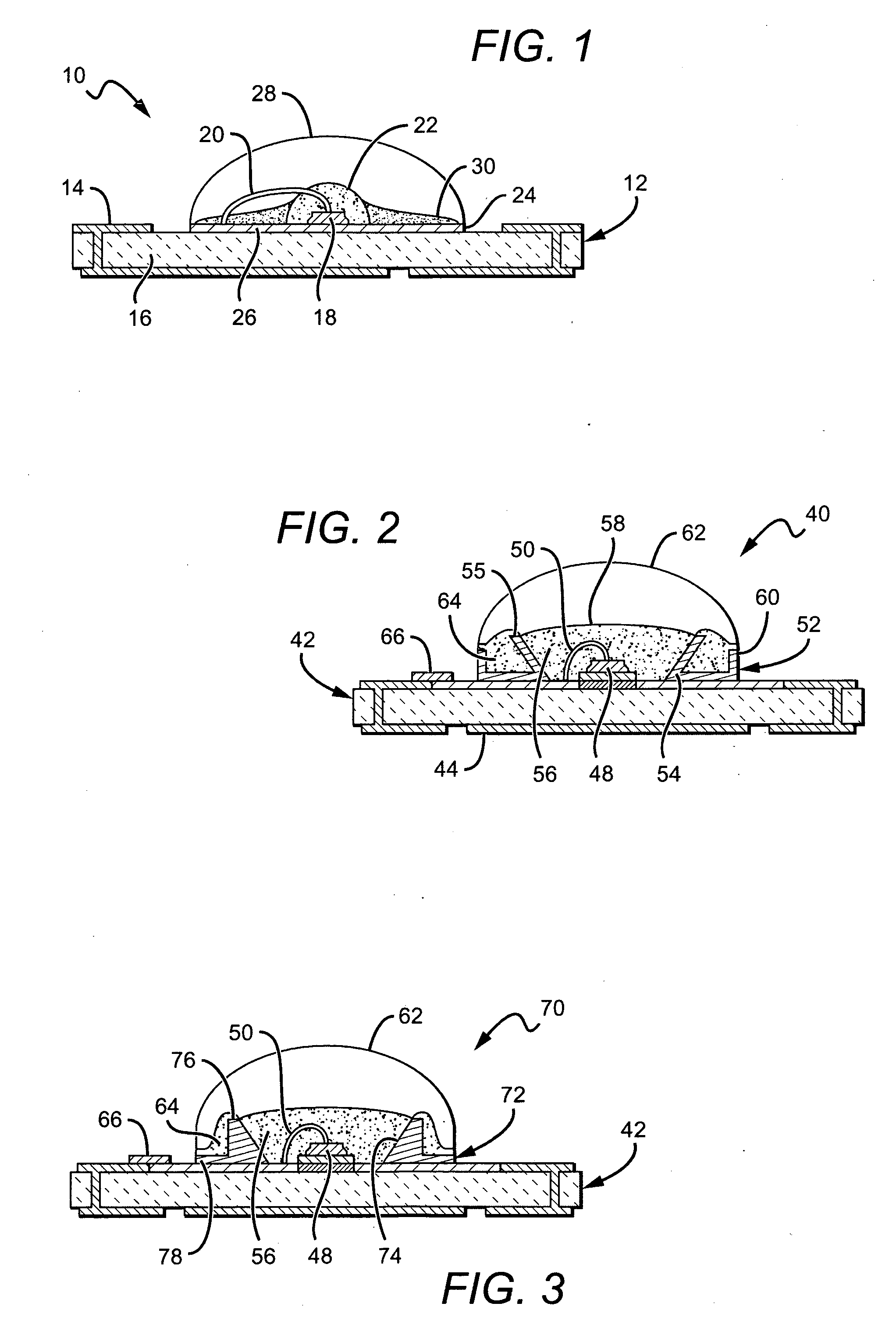
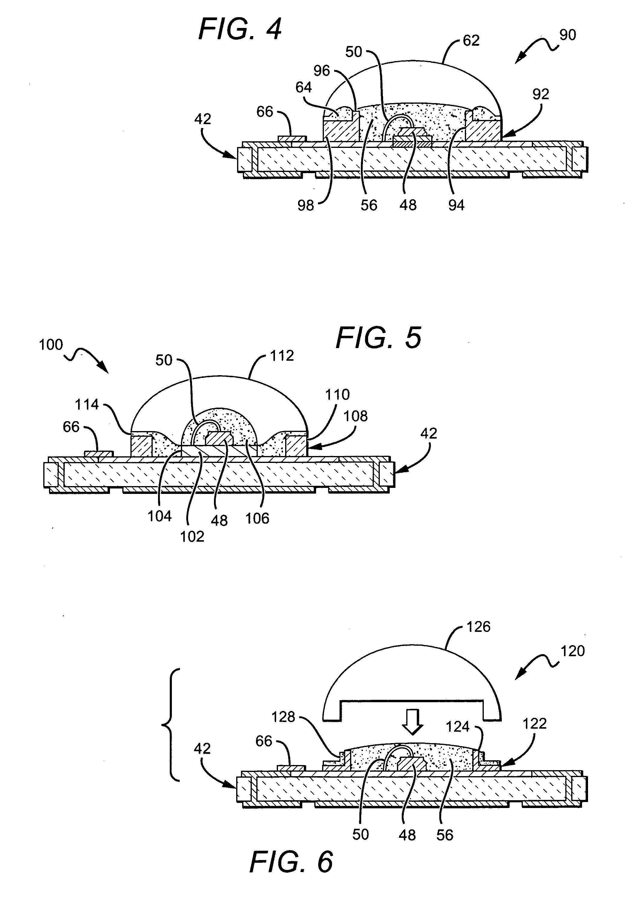
[0025]The present invention comprises a dispensed optical element or lens that may be fabricated directly on the LED lamp using common processing (e.g. dispensing) processes and equipment. The invention is particularly applicable to fabricating LED packages without the need for additional piece part (i.e. separately formed) lenses, although aspects of this invention can also be used with packages utilizing piece part fabricated lenses. The dispensed lens embodiments according to the present invention may be fabricated using a variety of available silicone or epoxy materials, allowing application to surface mount LED packages or arrays. Surface features, herein referred to as meniscus forming features or meniscus rings, may be included on the LED package to allow a substantially hemispherical lens to be formed from a liquid lens material by allowing formation of a meniscus. The term “substantially hemispherical” and related terms are meant to convey a variety of curved surfaces, incl...


PUM


Abstract

A light emitting diode (LED) package comprising a substrate with an LED chip mounted to the substrate and in electrical contact with it. An inner material covers the LED chip, and a lens covers the inner material with the lens material being harder than the inner material. An adhesive is arranged between the substrate and the lens to hold the lens to the substrate and to compensate for different coefficients of thermal expansion (CTE) between the lens and the remainder of the package. A method for forming an LED package comprises providing a substrate with a first meniscus ring on a surface of the substrate. An LED chip is mounted to the substrate, within the meniscus ring. An inner material is deposited over the LED chip, and a lens material in liquid form is deposited over the inner material. The lens material held in a hemispheric shape by the first meniscus feature and the lens material is cured making it harder than the inner material.

Description

BACKGROUND OF THE INVENTION[0001]1. Field of the Invention[0002]This invention relates to semiconductor light emitting diodes (LEDs) and more particularly to LED packages with optical elements.[0003]2. Description of the Related Art[0004]Light emitting diodes (LEDs) are solid state devices that convert electric energy to light, and generally comprise one or more active layers of semiconductor material sandwiched between oppositely doped layers. When a bias is applied across the doped layers, holes and electrons are injected into the active layer where they recombine to generate light. Light is emitted from the active layer and from all surfaces of the LED. The useful light is generally emitted in the direction of the LED's top surface.[0005]Conventional LEDs cannot generate white light from their active layers. One way to produce white light from conventional LEDs is to combine different colors from different LEDs. For example, the light from red, green and blue LEDs, or blue and ye...

Claims


Application Information

Patent Timeline
Patent Type & Authority Applications(United States)
IPC IPC(8): H01L33/00H01L33/48H01L33/50H01L33/58
CPCH01L33/486H01L33/56H01L33/58H01L2933/005H01L2224/48091H01L2924/00014
Inventor TARSA, ERICLEUNG, MICHAELBECERRA, MARYANNEKELLER, BERNDIBBETSON, JAMES
Owner CREELED INC
Why Eureka
Try Eureka